MicroBlaze Processor Reference Guide 34
UG984 (v2018.2) June 21, 2018 www.xilinx.com
Chapter 2: MicroBlaze Architecture
Exception Data Register (EDR)
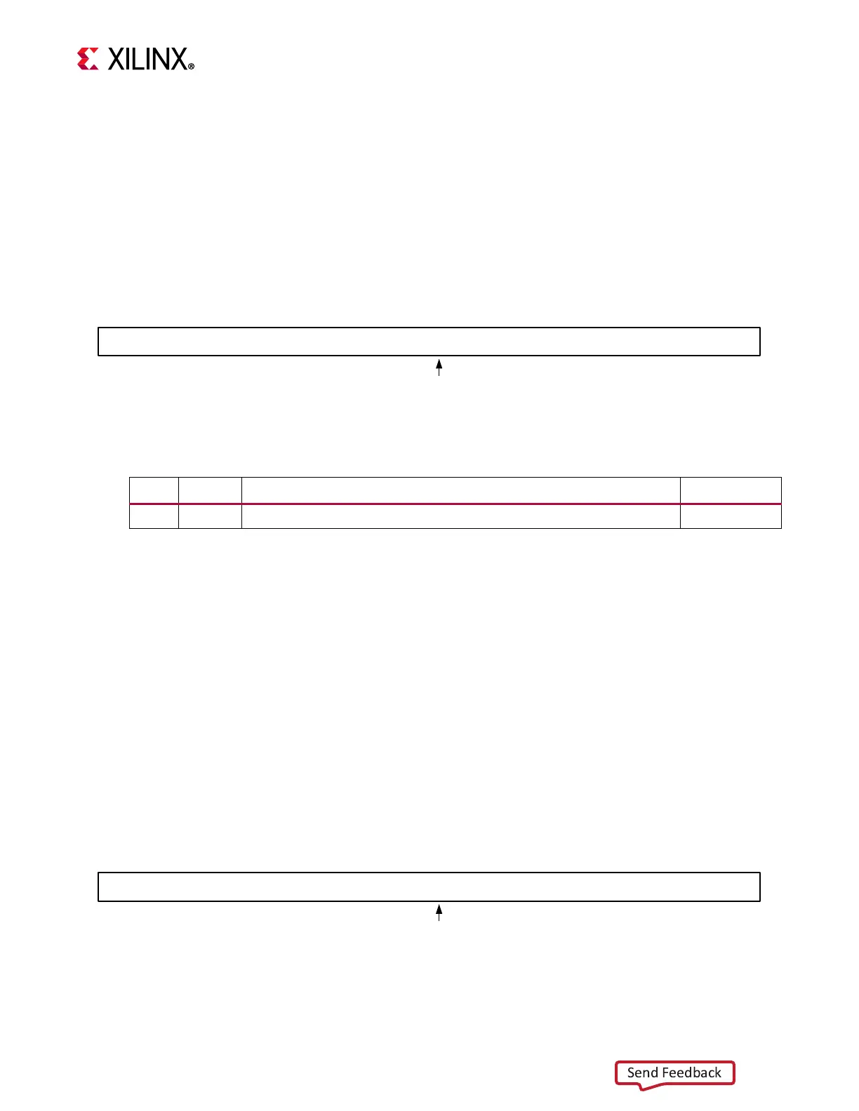
The Exception Data Register stores data read on an AXI4-Stream link that caused a stream
exception.
The contents of this register is undefined for all other exceptions. When read with the MFS
instruction, the EDR is specified by setting Sa = 0x000D. The following figure illustrates the
EDR register and
Table 2-15 provides bit descriptions and reset values.
Note: The register is only implemented if C_FSL_LINKS is greater than 0 and C_FSL_EXCEPTION
is set to 1.
Stack Low Register (SLR)
The Stack Low Register stores the stack low limit use to detect stack overflow. When the
address of a load or store instruction using the stack pointer (register R1) as rA is less than
the Stack Low Register, a stack overflow occurs, causing a Stack Protection Violation
exception if exceptions are enabled in MSR.
When read with the MFS instruction, the SLR is specified by setting Sa = 0x0800.
Figure 2-10 illustrates the SLR register and Table 2-16 provides bit descriptions and reset
values.
Note: The register is only implemented if stack protection is enabled by setting the parameter
C_USE_STACK_PROTECTION to 1. If stack protection is not implemented, writing to the register has
no effect.
Note: Stack protection is not available when the MMU is enabled (C_USE_MMU > 0). With the MMU
page-based memory protection is provided through the UTLB instead.
X-Ref Target - Figure 2-9
Figure 2-9: EDR
Table 2-15: Exception Data Register (EDR)
Bits Name Description Reset Value
0:31 EDR Exception Data Register 0x00000000
X-Ref Target - Figure 2-10
Figure 2-10: SLR