INSTALLATION
2-10
Markers
There are four markers. Three of them appear as TTL outputs on a D-type connector on the rear
panel, and all four appear as outputs or inputs on the 68-way LVDS connector also on the rear
panel. The markers can be generated internally or can be read from the LVDS connector. The
markers can be used to ‘mark’ specific sections of the modulated output; for example, the active
slot in a GSM frame. However, certain markers also have other functions as shown below.
Marker Use
1 General purpose / RF Burst control (0=off, 1=on)
2 General purpose / RF level select (A or B)
3 General purpose / Hop address trigger (+ve edge)
4 Not currently used
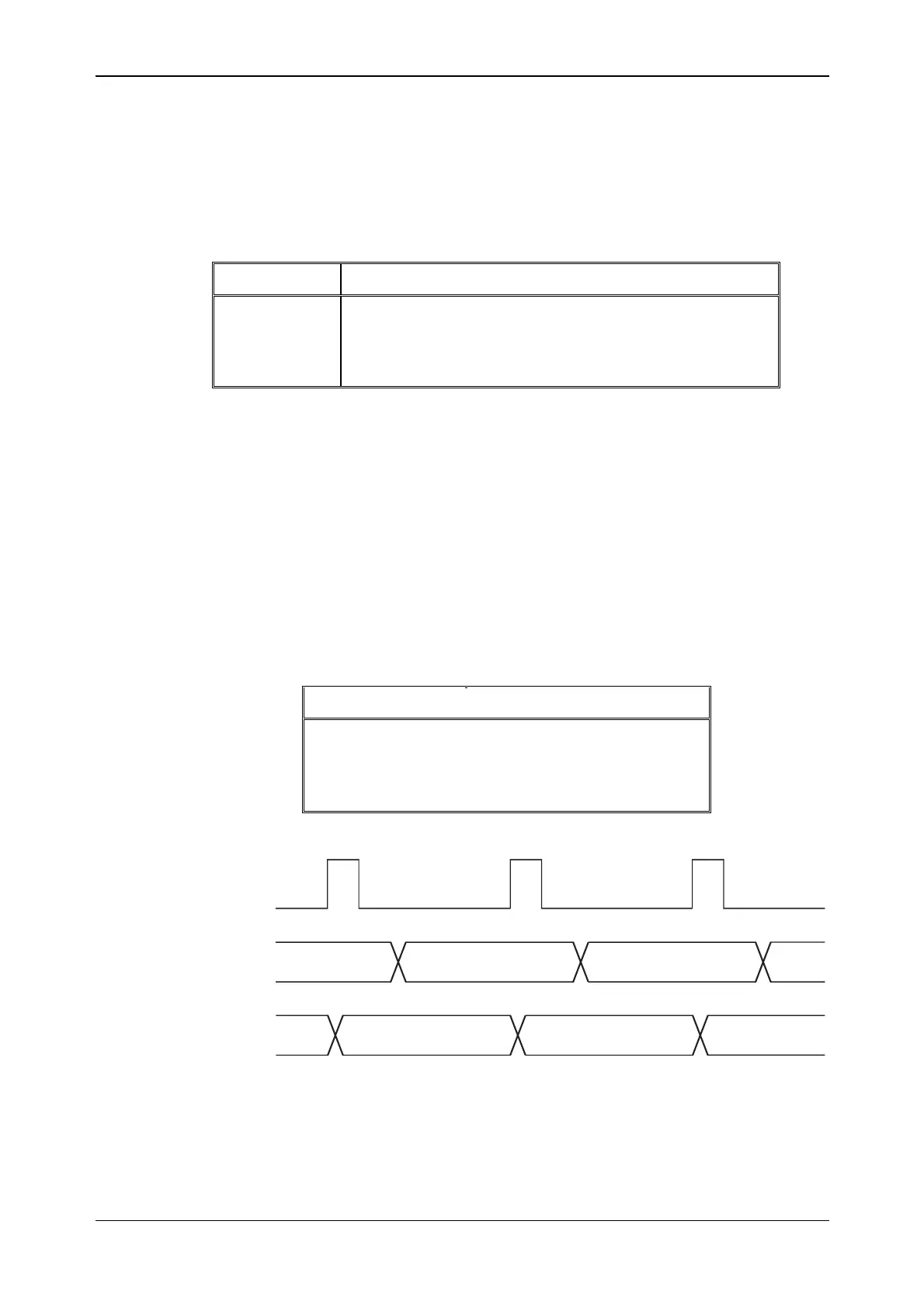
Hop address
There are five hop address lines and these appear as either outputs or inputs on the LVDS
connector. These five lines dictate which frequency offset is used from a lookup table that has
been set up internally. As shown above, the hop address is always latched on the rising edge of
Marker 3. The hop address can be generated internally by means of a counter. This counter is
also updated on the rising edge of Marker 3.
Example 1
Hop address is an input on the LVDS and the first four entries in the lookup table are:
Hop Address RF offset frequency
0 0 MHz
1 10 MHz
2
−30 MHz
3 50 MHz
MARKER3
HOP_ADDR
(input)
2
3
0 MHz 10 MHz
-30 MHz
1
0
RF frequency
offset
C5686