108
7647H–AVR–03/12
Atmel ATmega16/32/64/M1/C1
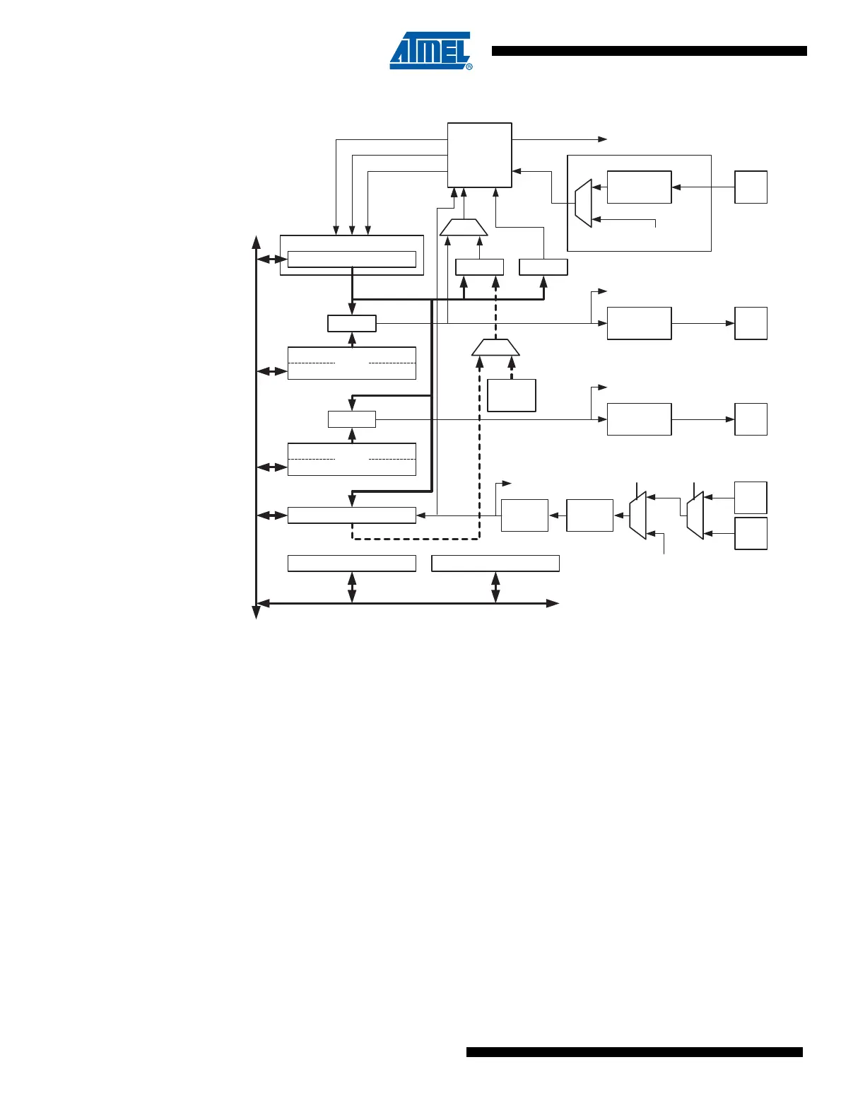
Figure 13-1. 16-bit Timer/Counter Block Diagram
(1)
Note: 1. Refer to Table on page 5 for Timer/Counter1 pin placement and description.
13.1.1 Registers
The Timer/Counter (TCNTn), Output Compare Registers (OCRnx), and Input Capture Register
(ICRn) are all 16-bit registers. Special procedures must be followed when accessing the 16-bit
registers. These procedures are described in the section “Accessing 16-bit Registers” on page
109. The Timer/Counter Control Registers (TCCRnx) are 8-bit registers and have no CPU
access restrictions. Interrupt requests (abbreviated to Int.Req. in the figure) signals are all visible
in the Timer Interrupt Flag Register (TIFRn). All interrupts are individually masked with the Timer
Interrupt Mask Register (TIMSKn). TIFRn and TIMSKn are not shown in the figure.
The Timer/Counter can be clocked internally, via the prescaler, or by an external clock source on
the Tn pin. The Clock Select logic block controls which clock source and edge the Timer/Counter
uses to increment (or decrement) its value. The Timer/Counter is inactive when no clock source
is selected. The output from the Clock Select logic is referred to as the timer clock (clk
T
n
).
Clock Select
Timer/Counter
DATA BUS
OCRnA
OCRnB
ICRn
=
=
TCNTn
Waveform
Generation
Waveform
Generation
OCnA
OCnB
Noise
Canceler
ICPnB
=
Fixed
TOP
Values
Edge
Detector
Control Logic
= 0
TOP BOTTOM
Count
Clear
Direction
TOVn
(Int.Req.)
OCnA
(Int.Req.)
OCnB
(Int.Req.)
ICFn (Int.Req.)
TCCRnA TCCRnB
Tn
Edge
Detector
( From Prescaler )
clk
Tn
ICPnA
ICPSEL1
0
1
RTG
AC1ICE
Analog Comparator 1
Interrupt