119
7647H–AVR–03/12
Atmel ATmega16/32/64/M1/C1
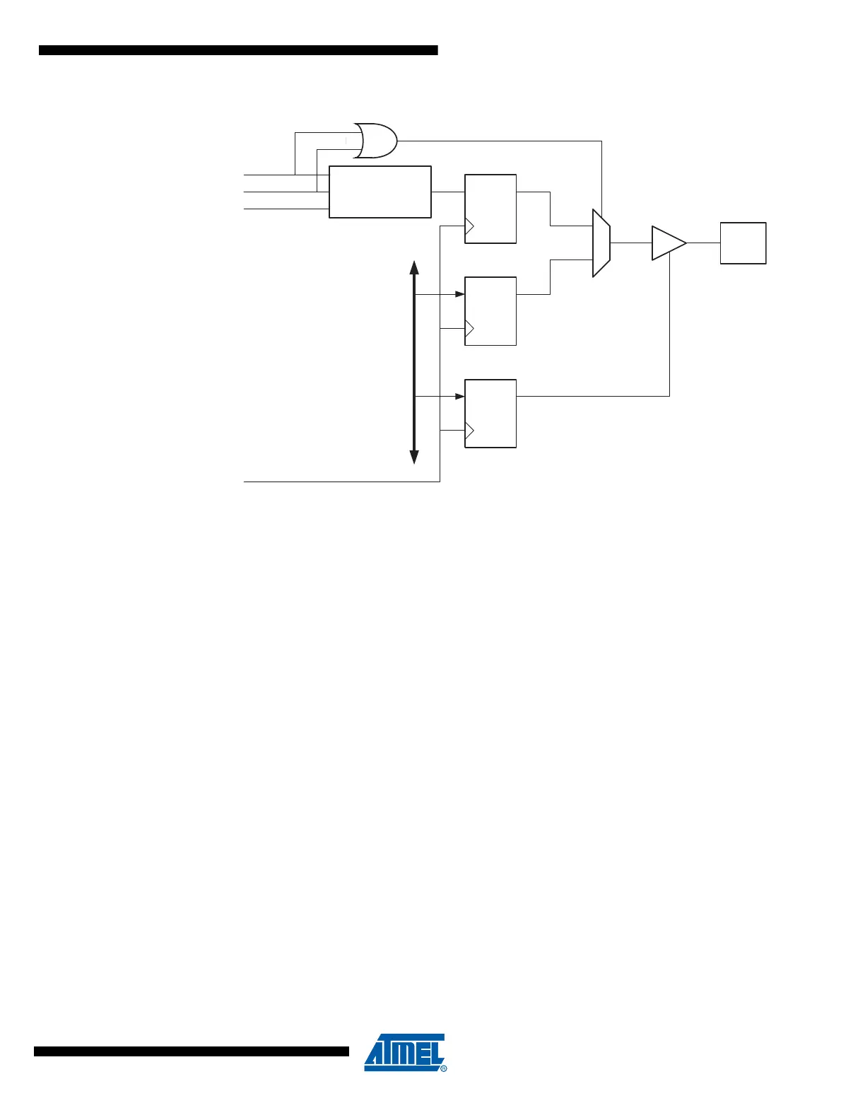
Figure 13-5. Compare Match Output Unit, Schematic
The general I/O port function is overridden by the Output Compare (OCnx) from the Waveform
Generator if either of the COMnx1:0 bits are set. However, the OCnx pin direction (input or out-
put) is still controlled by the Data Direction Register (DDR) for the port pin. The Data Direction
Register bit for the OCnx pin (DDR_OCnx) must be set as output before the OCnx value is visi-
ble on the pin. The port override function is generally independent of the Waveform Generation
mode, but there are some exceptions. Refer to Table 13-1, Table 13-2 and Table 13-3 for
details.
The design of the Output Compare pin logic allows initialization of the OCnx state before the out-
put is enabled. Note that some COMnx1:0 bit settings are reserved for certain modes of
operation. See “16-bit Timer/Counter Register Description” on page 130.
The COMnx1:0 bits have no effect on the Input Capture unit.
13.7.1 Compare Output Mode and Waveform Generation
The Waveform Generator uses the COMnx1:0 bits differently in normal, CTC, and PWM modes.
For all modes, setting the COMnx1:0 = 0 tells the Waveform Generator that no action on the
OCnx Register is to be performed on the next compare match. For compare output actions in the
non-PWM modes refer to Table 13-1 on page 130. For fast PWM mode refer to Table 13-2 on
page 130, and for phase correct and phase and frequency correct PWM refer to Table 13-3 on
page 131.
A change of the COMnx1:0 bits state will have effect at the first compare match after the bits are
written. For non-PWM modes, the action can be forced to have immediate effect by using the
FOCnx strobe bits.
PORT
DDR
DQ
DQ
OCnx
Pin
OCnx
DQ
Waveform
Generator
COMnx1
COMnx0
0
1
DATA BUS
FOCnx
clk
I/O

 Loading...


