131
7647H–AVR–03/12
Atmel ATmega16/32/64/M1/C1
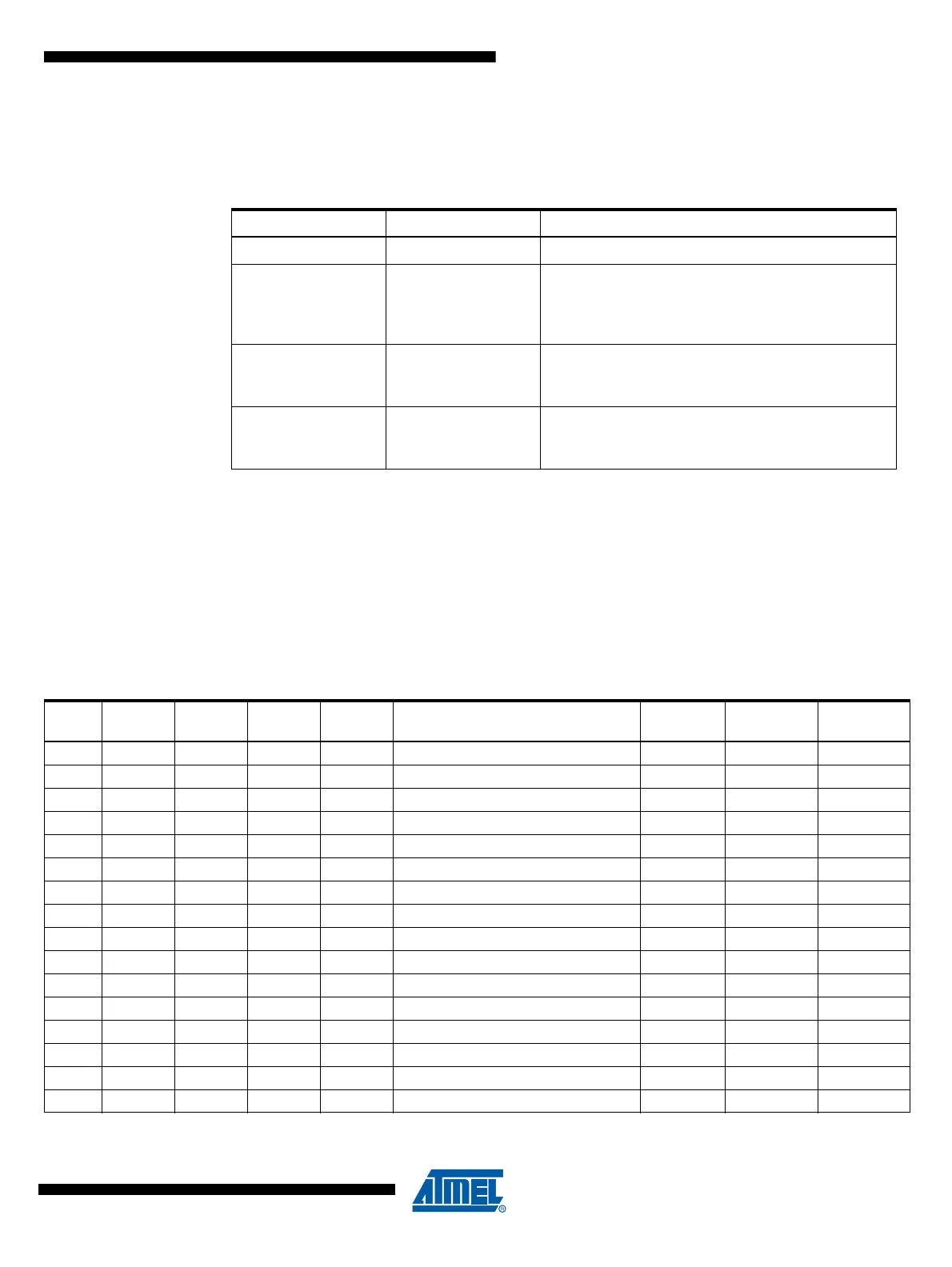
Table 13-3 shows the COMnx1:0 bit functionality when the WGMn3:0 bits are set to the phase
correct or the phase and frequency correct, PWM mode.
Note: 1. A special case occurs when OCRnA/OCRnB equals TOP and COMnA1/COMnB1 is set. See
“Phase Correct PWM Mode” on page 123. for more details.
• Bit 1:0 – WGMn1:0: Waveform Generation Mode
Combined with the WGMn3:2 bits found in the TCCRnB Register, these bits control the counting
sequence of the counter, the source for maximum (TOP) counter value, and what type of wave-
form generation to be used, see Table 13-4. Modes of operation supported by the Timer/Counter
unit are: Normal mode (counter), Clear Timer on Compare match (CTC) mode, and three types
of Pulse Width Modulation (PWM) modes. (See “16-bit Timer/Counter1 with PWM” on page
107.).
Note: 1. The CTCn and PWMn1:0 bit definition names are obsolete. Use the WGMn2:0 definitions. However, the functionality and
location of these bits are compatible with previous versions of the timer.
Table 13-3. Compare Output Mode, Phase Correct and Phase and Frequency Correct
PWM
(1)
COMnA1/COMnB1 COMnA0/COMnB0 Description
0 0 Normal port operation, OCnA/OCnB disconnected.
01
WGMn3:0 = 8, 9 10 or 11: Toggle OCnA on Compare
Match, OCnB disconnected (normal port operation).
For all other WGM1 settings, normal port operation,
OC1A/OC1B disconnected.
10
Clear OCnA/OCnB on Compare Match when
up-counting. Set OCnA/OCnB on Compare Match
when downcounting.
11
Set OCnA/OCnB on Compare Match when
up-counting. Clear OCnA/OCnB on Compare Match
when downcounting.
Table 13-4. Waveform Generation Mode Bit Description
(1)
Mode WGMn3
WGMn2
(CTCn)
WGMn1
(PWMn1)
WGMn0
(PWMn0) Timer/Counter Mode of Operation TOP
Update of
OCRnx at
TOVn Flag
Set on
0 0 0 0 0 Normal 0xFFFF Immediate MAX
1 0 0 0 1 PWM, Phase Correct, 8-bit 0x00FF TOP BOTTOM
2 0 0 1 0 PWM, Phase Correct, 9-bit 0x01FF TOP BOTTOM
3 0 0 1 1 PWM, Phase Correct, 10-bit 0x03FF TOP BOTTOM
4 0 1 0 0 CTC OCRnA Immediate MAX
5 0 1 0 1 Fast PWM, 8-bit 0x00FF TOP TOP
6 0 1 1 0 Fast PWM, 9-bit 0x01FF TOP TOP
7 0 1 1 1 Fast PWM, 10-bit 0x03FF TOP TOP
8 1 0 0 0 PWM, Phase and Frequency Correct ICRn BOTTOM BOTTOM
9 1 0 0 1 PWM, Phase and Frequency Correct OCRnA BOTTOM BOTTOM
10 1 0 1 0 PWM, Phase Correct ICRn TOP BOTTOM
111011PWM, Phase Correct OCRnA TOP BOTTOM
12 1 1 0 0 CTC ICRn Immediate MAX
13 1 1 0 1 (Reserved) – – –
141110Fast PWM ICRnTOPTOP
151111Fast PWM OCRnATOPTOP