238
7647H–AVR–03/12
Atmel ATmega16/32/64/M1/C1
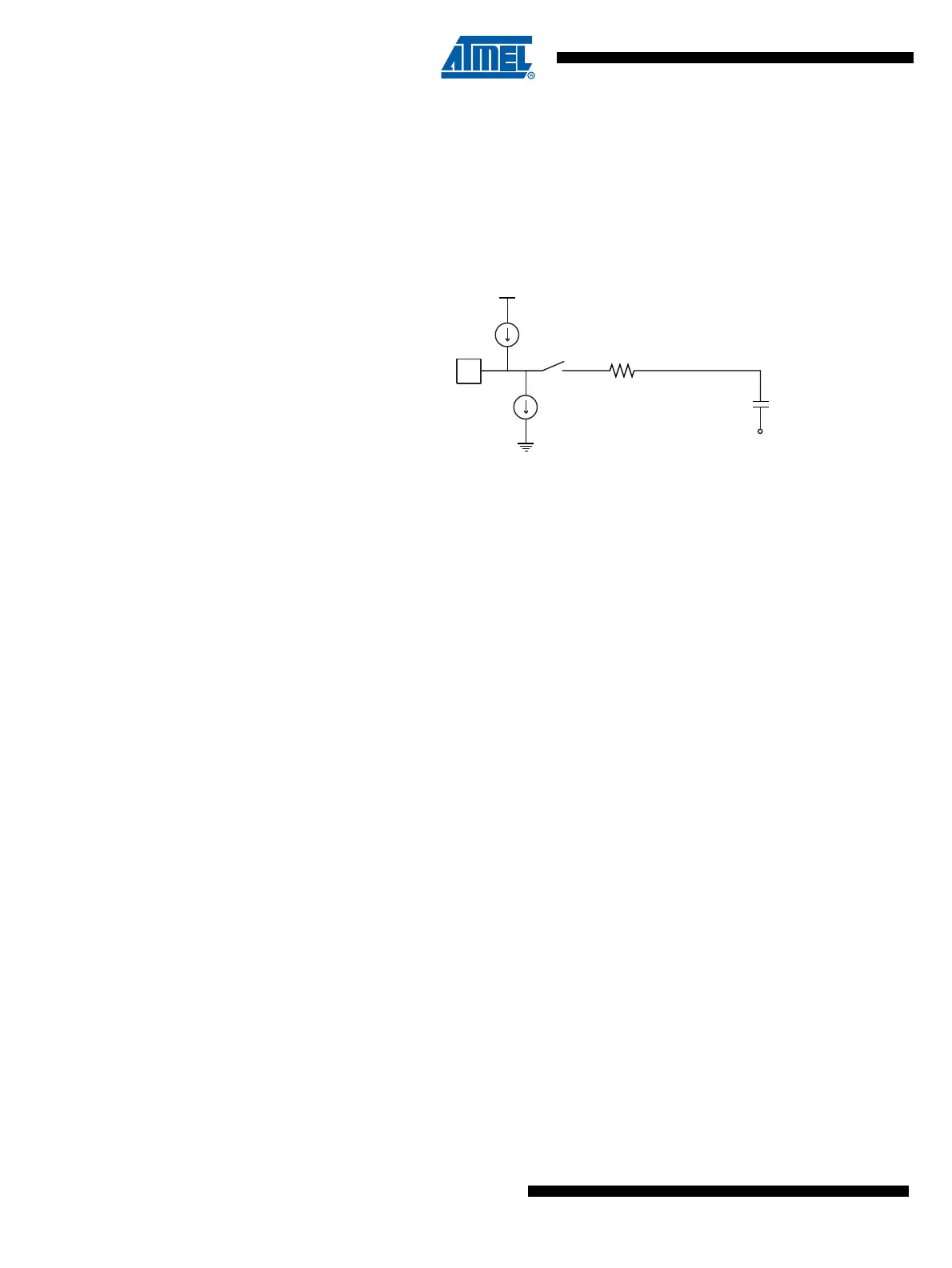
If differential gain channels are used, the input circuitry looks somewhat different, although
source impedances of a few hundred kΩ or less is recommended.
Signal components higher than the Nyquist frequency (f
ADC
/2) should not be present for either
kind of channels, to avoid distortion from unpredictable signal convolution. The user is advised
to remove high frequency components with a low-pass filter before applying the signals as
inputs to the ADC.
Figure 18-8. Analog Input Circuitry
18.6.2 Analog Noise Canceling Techniques
Digital circuitry inside and outside the device generates EMI which might affect the accuracy of
analog measurements. If conversion accuracy is critical, the noise level can be reduced by
applying the following techniques:
1. Keep analog signal paths as short as possible. Make sure analog tracks run over the
analog ground plane, and keep them well away from high-speed switching digital
tracks.
2. The AVCC pin on the device should be connected to the digital VCC supply voltage via
an RC network (R = 10Ω max, C = 100 nF).
3. Use the ADC noise canceler function to reduce induced noise from the CPU.
4. If any ADC port pins (PB[7:2], PC[7:4], PD[6:4], PE[2]) are used as digital outputs, it is
essential that these do not switch while a conversion is in progress.
18.6.3 Offset Compensation Schemes
The gain stage has a built-in offset cancellation circuitry that nulls the offset of differential mea-
surements as much as possible. The remaining offset in the analog path can be measured
directly by shortening both differential inputs using the AMPxIS bit with both inputs unconnected.
(See “Amplifier 0 Control and Status register – AMP0CSR” on page 254., See “Amplifier 1 Con-
trol and Status register – AMP1CSR” on page 255.and See “Amplifier 1 Control and Status
register – AMP1CSR” on page 255.). This offset residue can be then subtracted in software from
the measurement results. Using this kind of software based offset correction, offset on any chan-
nel can be reduced below one LSB.
18.6.4 ADC Accuracy Definitions
An n-bit single-ended ADC converts a voltage linearly between GND and V
REF
in 2
n
steps
(LSBs). The lowest code is read as 0, and the highest code is read as 2
n
-1.
Several parameters describe the deviation from the ideal behavior:
• Offset: The deviation of the first transition (0x000 to 0x001) compared to the ideal transition
(at 0.5 LSB). Ideal value: 0 LSB.
ADCn
I
IH
1..100 kΩ
C
S/H
= 14 pF
V
CC
/2
I
IL