Parameter
structure
Keypad and
display
Parameter
x.00
Parameter
description format
Advanced parameter
descriptions
Macros
Serial comms
protocol
Electronic
nameplate
Performance RFC mode
Menus 15 to 17
SM-I/O PELV
Unidrive SP Advanced User Guide 305
Issue Number: 10 www.controltechniques.com
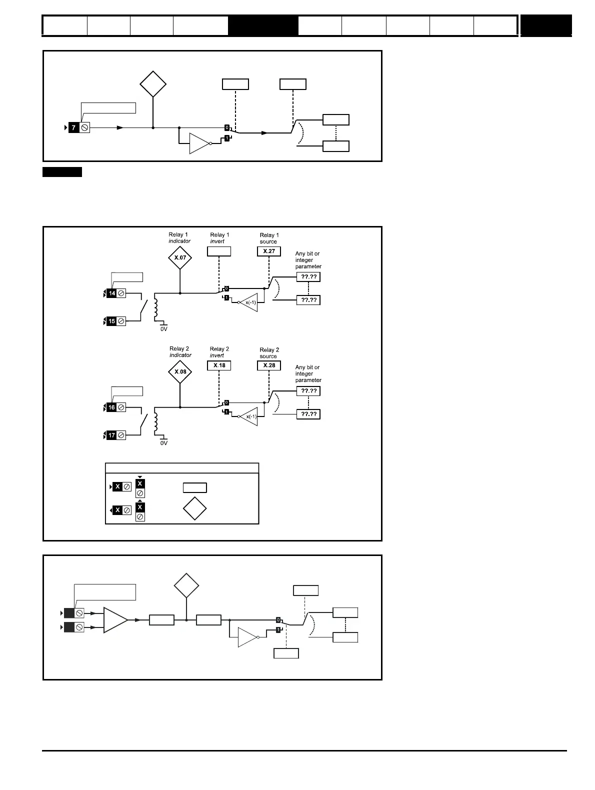
Figure 5-20 SM-I/O PELV digital input logic diagram
The performance of the freeze input is highly dependant upon the quality of the signal driving it. If negative edge triggering is used then care should
be taken to ensure that the input is actively pulled low via low impedance. If positive edge triggering is used then care should be taken to ensure that
the input is actively pulled high, or pulled high via a suitably low pull-up resistance.
Figure 5-21 SM-I/O PELV relay logic diagram
Figure 5-22 SM-I/O PELV analog input logic diagram (current mode)
X.25
x(-1)
X.15X.05
T7 digital input 5
T7 digital
input 5 state
T7 digital
input 5 invert
T7 digital input 5
destination
Relay 2
X.17
Relay 1
0.XX
0.XX
Key
Read-write (RW)
parameter
Read-only (RO)
parameter
Input
terminals
Output
terminals
The parameters are all shown at their default setting
X.43
Analog
input 1
destination
x(-1)
X.42
Analog input 1
invert
X.40
Analog input 1
Analog input
1 level
8
9
+
_
X.38
Analog
input 1
mode selector
 Loading...