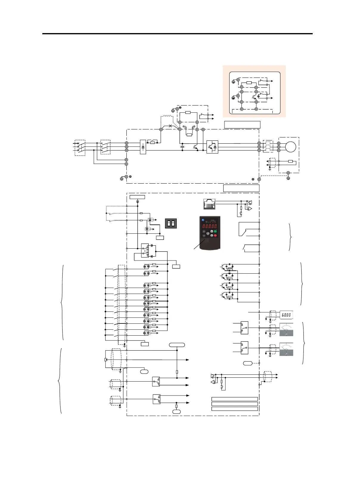
Pulse output
FMP
CM
Voltage output
(0 to ±10 V DC)
PLC
FWD
REV
X1
X2
X3
X4
X5
CM
EN1
SINK
SOURCE
EN2
0V
+24VDC
FM1
11
0V
Data transfer/receipt
DX+
DX-
SW2
SW1
Analog input/output common
SW4
IO1
VO1
11
12
13
+10VDC
0V
3
2
1
X6
X7
X8
X9
V2
(+)
(-)
V2
SW5
PTC/NTC
Braking resistor (DBR)
DC reactor
(DCR)
DB N(-)
P(+)
P1
U
V
W
U
V
W
M
3~
L1/R
L2/S
L3/T
Magnetic
contactor
(MC)
Circuit breaker
(MCCB) or earth
leakage circuit
breaker (ELCB)
Power supply
200 V system
200 to 240 V
50/60 Hz
400 V system
380 to 480 V
50/60 Hz
G
P DB
2
1
(CM)
(THR)
(G)
Thermistor
to[11]
to[V2]
Thermal
overload
relay
)
R0
T0
Control power
auxiliary input
G
E
Gro unding terminal
Motor
Variable resistor power supply
RJ-45 connector for keypad
SW3
RS-485
communicati
on port 1
USB connector
RS-485
communication
port 2
(terminal block)
(SD)
Voltage output
(0 to ±10 V DC)
FM2
Current output
(4(0) to 20 mA DC)
IO2
VO2
SW6
Analog meter
11
11
Run forward command
Run reverse command
Multistep frequency selection
(0 to 1 step)
Multistep frequency selection
(0 to 3 step)
Multistep frequency selection
(0 to 7 step)
Digital input common
Multistep frequency selection
(0 to 15 step)
Acceleration/deceleration time
selection (2 steps)
Acceleration/deceleration time
selection (4 steps)
Self-hold selection
Coast to stop command
Alarm (error) reset
Enable
(STO) inpu t
Control circuit
Main circuit
Grounding
terminal
*1
*2
*3
*5
*6
*7
*8
*11
*11
*11
*11
*11
*11
*9
*12
C1
(+)
(-)
Y3
Y4
CMY
30C
30B
30A
Batch alarm output
Y5C
Y5A
AX terminal function
Y2
Y1
Runnin g
Motor overload warning
Common termina l
Freque ncy (speed) arrival
Frequency (speed) detection
*9
*9
Analog meter
CM
V3
SW8
C1
0V
DBR
N(-)P(+)
P
DB
2
1
(CM)
(G)
2
1
(THR)
P(+)
N(-)
Braking resistor
Braking unit
(BU)
(G)
P(+)R
DB
*6
*13
*15
*15
*15
SW7
DBR
ON
*12
+
OFF
0V
0V
*15
PLC
Digital input
Analog input
Voltage input for setting
0 to ±10 V DC
Voltage input for setting
0 to ±10 V DC
PTC/NTC input
Voltage input for setting
0 to ±10 V DC
Analog input/output common
Current input for setting
4(0) to 20 mA DC
Option card connection connector A
Option card connection connector B
Option card connection connector C
Analog output
Curren t output
(4(0) to 20 mA DC)
Transistor output
Contact output
*15*11
*15
*16
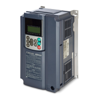
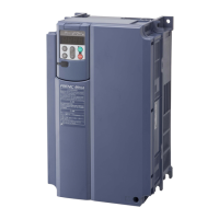
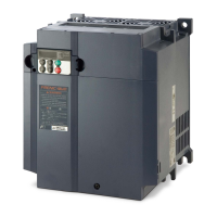
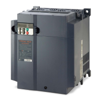
Fig. 2.2‑1 Basic connection diagram
 Loading...