Development Board Features
Development Kit User’s Manual 33
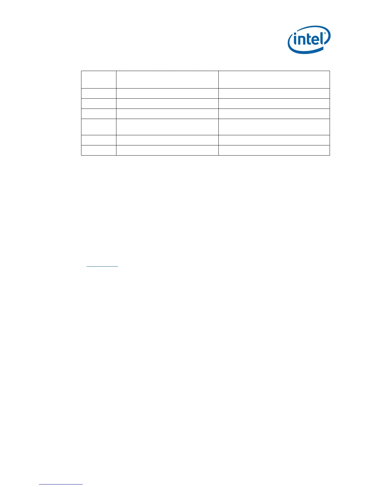
Table 8. PCI Express Ports
ICH9M
PCIe Port
Default Destination Optional Destination
1 PCIe Slot 1 (J6B1) PCIe Docking (1
st
lane)
2 PCIe Slot 2 (J6D1) (in-line with Slot 1) PCIe Docking (2
nd
lane)
3 PCIe Slot 3 (J8B3)
4 PCIe Slot 4 (J8D1) (in-line with Slot 3) C-link south routed to this slot. WLAN card
support through Upham3 Add-in card
5 PCIe Slot 5 (J7B1)
6 (GLCI) Intel 82567 LAN Muxed with PCIe slot5 (only for testing)
Slot 4 also supports controller link. Upon a net detect event, Slot 4 gets a switched
Auxiliary 3.3 V supply.
3.6.11 PCI Slots
The reference board does not have any PCI slots on the motherboard. Three 5V PCI
slots are supported via the Thimble Peak PCI Extension Card.
3.6.11.1 PCI Gold-Fingers
A gold-finger connector (S9B1) is also supplied on the development board, which
allows an external PCI expansion board, Thimble Peak 2, to connect to it. Thimble
Peak 2 has three additional PCI slots allowing the user greater expansion. See
Appendix A
for more information on the Thimble Peak 2 add-in card.
3.6.12 On-Board LAN
The development board provides 10/100/1000 LAN through EU8A1. Intel ® 82567 is
used on the reference board. The 82567 component is connected to the ICH9M chipset
through the LAN Connect Interface (LCI) and supports 10/100Mbps link. The same
device is connected through GLCI interface and supports 1000Mbps link. 82567
connect to an RJ45 connector at J5A1 with built in magnetic decoupling.
3.6.13 Serial Peripheral Interface (SPI)
The Serial Peripheral Interface on ICH9M can be used to support two compatible flash
devices (U8C1 (or U8B2), U8C4 (or U8C3)). Both the SPI devices supports for multi-
package (SOIC-8 and SOIC-16) device. The SOIC-8 package (U8C1 & U8C4) would
support 16 Mb SPI flashes, while the SOIC-16 package (U8B2 & U8C3) will support
32Mb or higher SPI flash. Unified BIOS code (BIOS+ IAMT+ LAN) resides in these two
SPI devices.
Note: Out of the SOIC-8 and SOIC-16 footprints supported on the board only one of these
can be used at a time and on the board the Footprint is arranged one over the other.
By default, U8C1 (16Mb on CS#0) and U8C4 (16Mb on CS#1) will be stuffed.