Document Number: 320249-001
Appendix C Programming System
BIOS Using a Flash Programming
Device
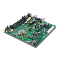
The BIOS for the Silver Cascade development board is in two non-removable flash
devices. The flash can be programmed using a bootable DOS device, or through a
special BIOS programming device that connects to header J8D2 on the board. One
such programming device is the Dediprog SF100 available from the manufacturer at
www.dediprog.com
.
The Silver Cascade development board required the use of a 2 partition SPI image for
SPI-0 and SPI-1 respectively. The descriptors are stored on SPI-0 while the BIOS is on
SPI-1.
To program the flash using a flash programming device:
3. Setup the hardware and software of the flash programming device on a host
system according to the manufacturers instructions.
4. Obtain the latest BIOS image (separated into two .bin files). Store the image files
on the host system.
5. Disconnect the power supply of the development board.
6. Connect the programming device to the development board at J8D2.
7. Set jumpers J9C1 and J9D1 at 1-2.
8. Set jumper J8C1 at 1-2 for SPI-0. Erase the existing image and flash the .bin
image corresponding to SPI-0.
9. Set the jumper J8C1 at 2-3 for SPI-1. Erase the existing image and flash the .bin
image corresponding to SPI-1.
10. Once the programming is successful on both the SPI, set J8C1, J9C1 and J9D1 to
1-X.
11. Remove the flash programmer connector from J8D2.
12. Set the jumper J8H1 at 1-X for booting from the SPI.
§

 Loading...


