CX950 Hardware Reference Manual
18-2
3021M100-002
18.1 DIM Components
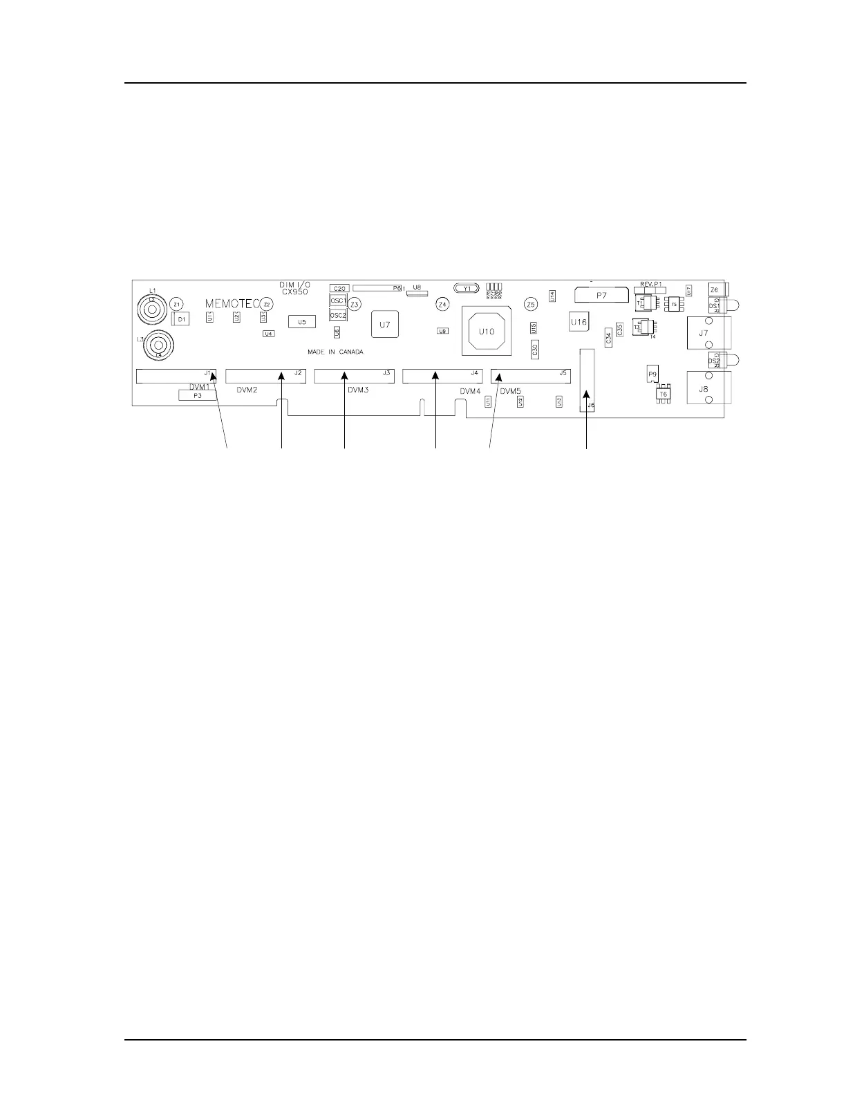
This section describes the major components of the DIM. The physical layout of
the components is shown in Figure 18-1. Figure 18-2 provides a functional block
diagram of the module.
18.1.1 CX950 I/O Bus
The CX950 I/O bus carries the address bus, data bus, and clocking/control signals
from the motherboard CPU to the DIM. Buffers interface the local buses to the
CX950 I/O bus. Connection of the I/O bus to the motherboard is via a 120-pin
card edge connector.
18.1.2 Time Slot Interchanger
The Time Slot Interchanger (TSI) interconnects the T1/E1 lines to the five DVP
daughterboards for voice channels and to the motherboard CPU for data channels.
The TSI also interconnects all the Digital Interface cards through the H.100/H.110
bus via the motherboard. The TSI can be used to interconnect both T1/E1 ports to
eachother.
18.1.3 T1/E1 Framer
The T1/E1 Framer accepts and generates coding such as Binary 8-Zero
Substitution (B8ZS), High Density Bipolar order 3 (HDB3), and Alternate-Mark-
Inversion (AMI) on the T1/E1 line interface. It handles the framing and
synchronization of T1/E1 lines.
Figure 18-1 DIM (without daughterboards)
Digital Voice Processor (DVP) slots (processors not shown) STEP