CX950 Hardware Reference Manual
4-8
3021M100-002
DTE
When configured as a DTE device, the port transmits DTR, RTS and ETXC and
receives DCD, DSR and CTS and the synchronous clock signals TXC and RXC
from the attached DCE.
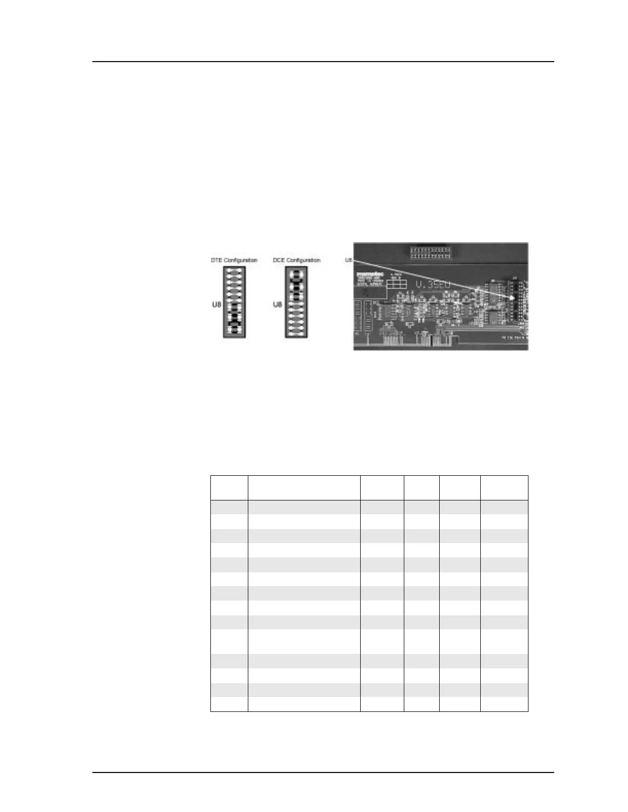
A jumper bank socketed at U8 provides DTE/DCE configuration. Permanent
metal bands on the top surface of the jumper bank strap signals according to DCE/
DTE requirements. The orientation of the jumper bank determines whether the
port will be DTE or DCE. Rotating the jumper 180° changes the port from one
kind of device to the other, as illustrated below.
4.2.4 V.35EU Serial I/O Card Signal Handling
Signaling through the V.35EU Serial I/O Card’s port complies fully with the
ITU-T’s (CCITT) V.35 standard for an M-34 block connector.
Figure 4-6 V.35EU DTE/DCE Configuration Jumper
Table 4-2 Signal Pin-Outs for V.35EU Port
V.35EU
Signal
Circuit Function ITU-T
M-34
Pin No.
Signal
DTE
Direction-
DCE
F. GND Protective Ground 101 A n/a n/a
TXDA Transmitted Data (Set A) 103-A P Out In
RXDA Received Data (Set A) 104-A R In Out
RTS Request to Send 105 C Out In
CTS Clear to Send 106 D In Out
DSR Data Set Ready 107 E In Out
S. GND Signal Ground 102 B n/a n/a
DCD Data Carrier Detect 109 F In Out
RXCB Receiver Clock (Set B) 115 X In Out
ETXCB
External Transmitter Clock
(Set B)
113-B W Out In
TXCB Transmitter Clock (Set B) 114-B AA In Out
TXDB Transmitted Data (Set B) 103-B S Out In
TXCA Transmitter Clock (Set A) 114-A Y In Out
RXDB Received Data (Set B) 104-B T In Out