CX950 Hardware Reference Manual
6-2
3021M100-002
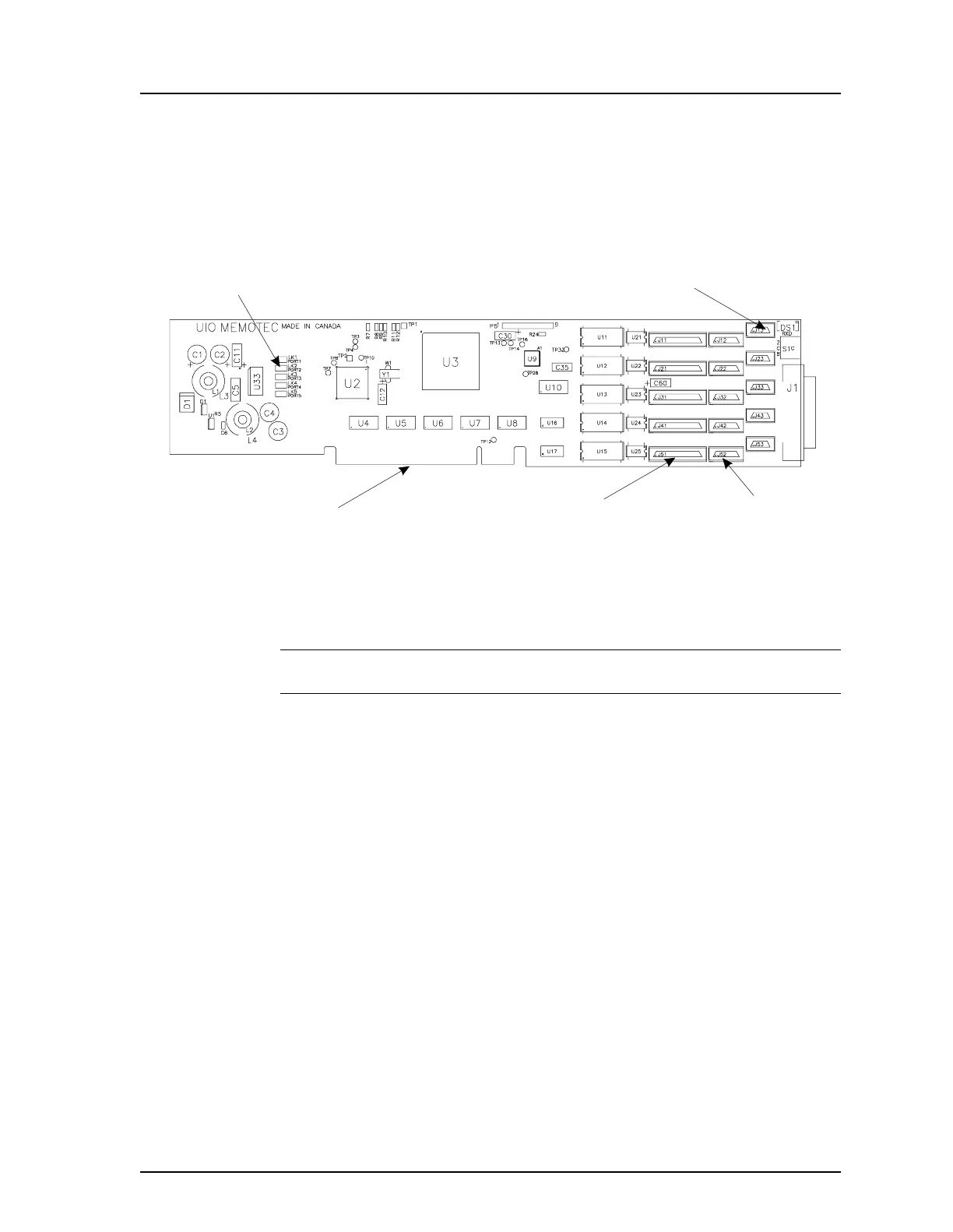
6.1 Universal I/O Card Components
This section describes the major components of the Universal I/O card. Th
physical layout of the components is shown in Figure 6-1. Figure 6-2 provides a
functional block diagram of the card.
WARNING:
Do not tamper with the LK Jumpers on this card.
6.1.1 CX950 I/O Bus
The CX950 I/O bus carries the address bus, data bus, and clocking/control signals
from the motherboard CPU to the Universal I/O card. Transceivers interface th
local buses to the CX950 I/O bus. Connection of the I/O bus to the motherboard is
via a 120-pin card edge connector.
6.1.2 Communications Controller
The MC68EN360, located at U3, is a Quad Universal Integrated Communications
Controller (QUICC) containing four Serial Communication Controllers (SCCs)
which serve ports 2 to 5. The SCC for Port 1 is provided by the motherboard.
An additional QUICC is required when Universal I/O cards are installed in slots 5
to 8. This QUICC is located on the Serial Expansion Module (SEM) which is a
plug-in card inserted into a 144-pin SODIMM connector on the motherboard on
U3.
Figure 6-1 Universal I/O Card
to motherboard expansion slots
edge connector
confi
uration connector
physical interfaceDTE/DCE port
confi
uration connector
LK Jumpers (LK1 to LK5)
configuration connector
clock source