CX950 Hardware Reference Manual
4-12
3021M100-002
4.3.4 V.35H Serial I/O Card Signal Handling
Signaling through the V.35H Serial I/O Card’s port complies fully with the ITU-
T’s (CCITT) V.35 standard. Signaling, however, occurs through a DB-25
connector rather than an M-34 block connector.
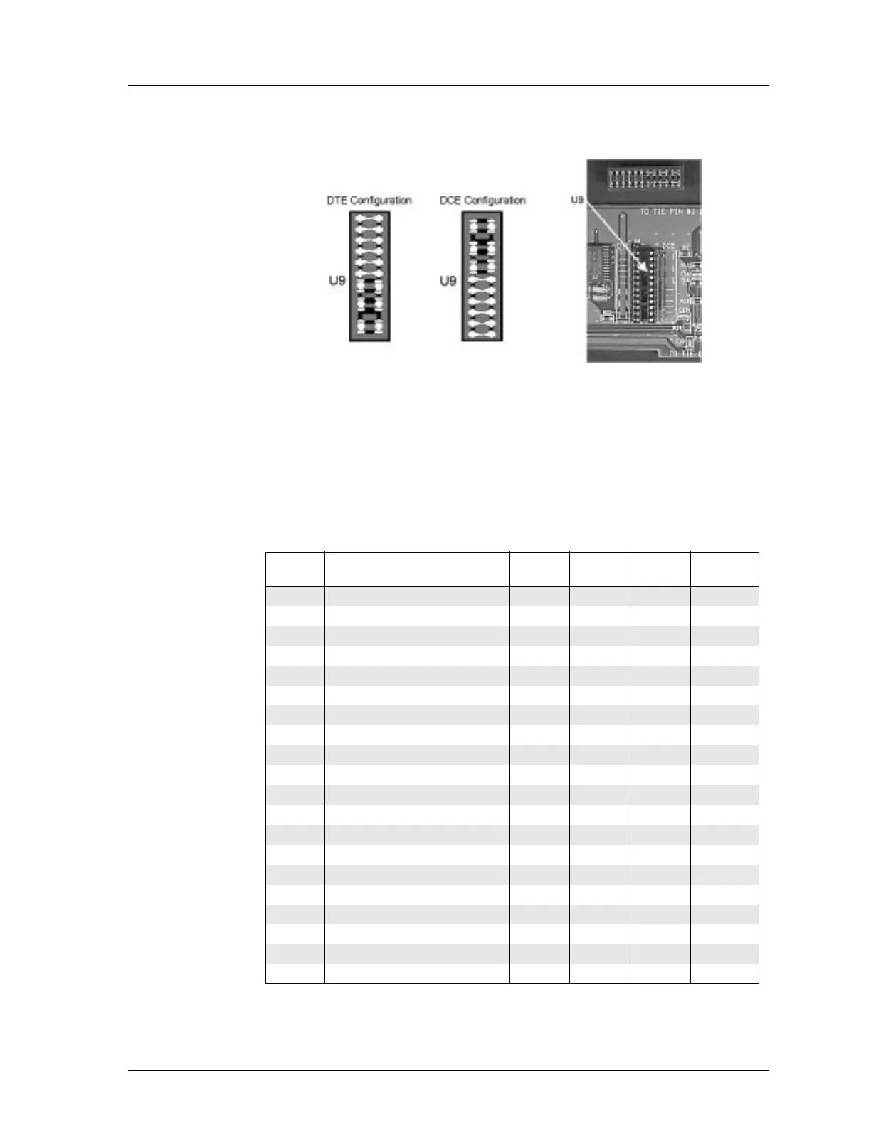
Figure 4-9 V.35H DTE/DCE Configuration Jumpe
Table 4-3 Signal Pin-Outs for V.35H Port
V.35H
Signal
Circuit Function ITU-T
DB-25
Pin No.
Signal
DTE
Direction
DCE
F. GND Protective Ground 101 1 n/a n/a
TXDA Transmitted Data (Set A) 103-A 2 Out In
RXDA Received Data (Set A) 104-A 3 In Out
RTS Request to Send 105 4 Out In
CTS Clear to Send 106 5 In Out
DSR Data Set Ready 107 6 In Out
S. GND Signal Ground 102 7 n/a n/a
DCD Data Carrier Detect 109 8 In Out
RXCB Receiver Clock (Set B) 115 9 In Out
*Unassigned 10 n/a n/a
ETXCB External Transmitter Clock (Set B 113-B 11 Out In
TXCB Transmitter Clock (Set B) 114-B 12 In Out
*Unassigned 13 not used not used
TXDB Transmitted Data (Set B) 103-B 14 Out In
TXCA Transmitter Clock (Set A) 114-A 15 In Out
RXDB Received Data (Set B) 104-B 16 In Out
RXCA Receiver Clock (Set A) 115-A 17 In Out
*Unassigned 18 not used not used
*Unassigned 19 not used not used
DTR Data Terminal Ready 108 20 Out In