98 LD-250 Platform User's Guide 20472-000 Rev B
6.2 Payload Bay Connections - LD-250 Core
Callout Side 1 (Left)
I/O Connector
Callout Side 2 (Right)
User-Supplied Equipment
A Equivalent Circuit F Terminal Block
B Input Bank 1 G Typical User Input Signal
C Input Bank 2 H Part Present Sensor
D Input Bank 3 I Bank 1 configured for sinking (NPN) inputs
E Input Bank 4 J Bank 4 configured for sinking (PNP) inputs
NOTE: You can use all input signals for either sinking or sourcing con-
figurations.
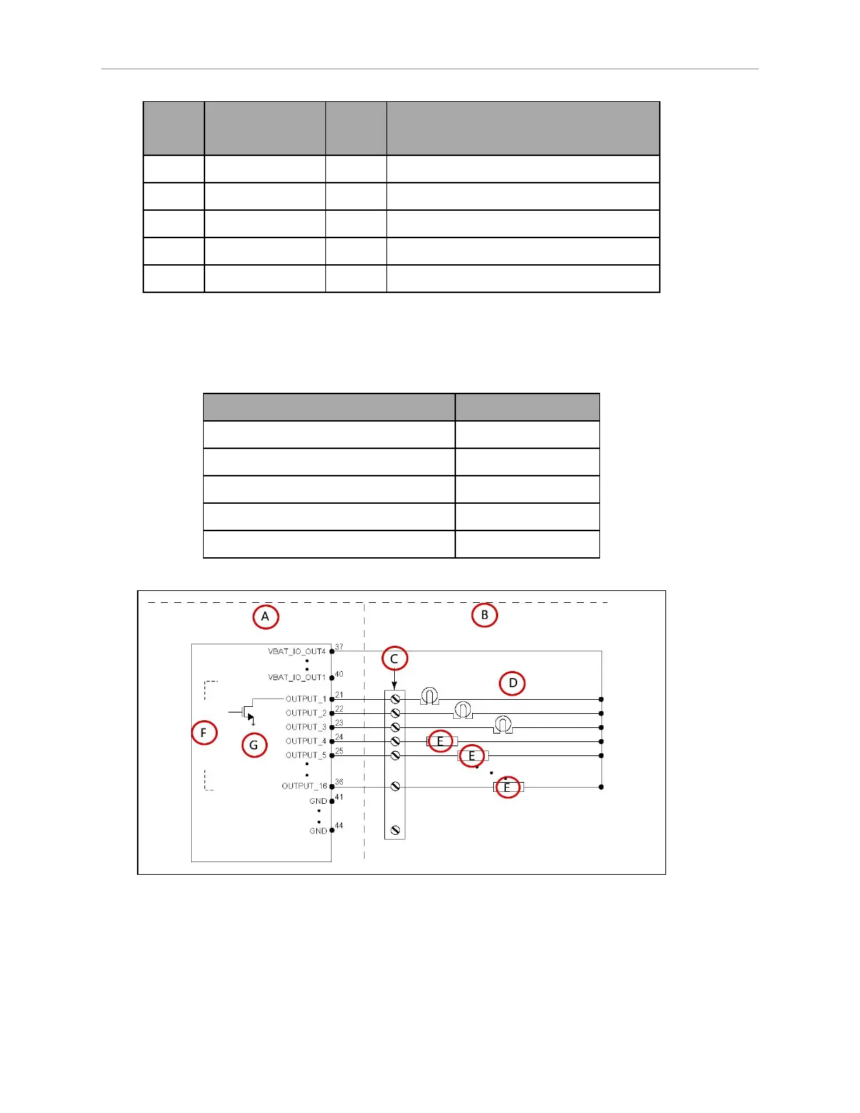
Table 6-2 Digital Output Specifications
Parameter Value
Power supply voltage range 5 - 30 VDC
Operational current range, per channel I
out
≤ 500 mA
ON state resistance (I
out
= 0.5 A) R
on
≤ 0.14 Ω @ 85°C
Output leakage current I
out
≤ 5 μA
DC short circuit current limit 0.7 A ≤ I
LIM
≤ 1.7 A
Figure 6-3 Typical Digital Output Wiring Example