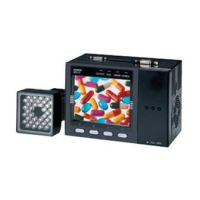
Internal Specifications
160
ZFX-C User’s Manual
Internal Specifications
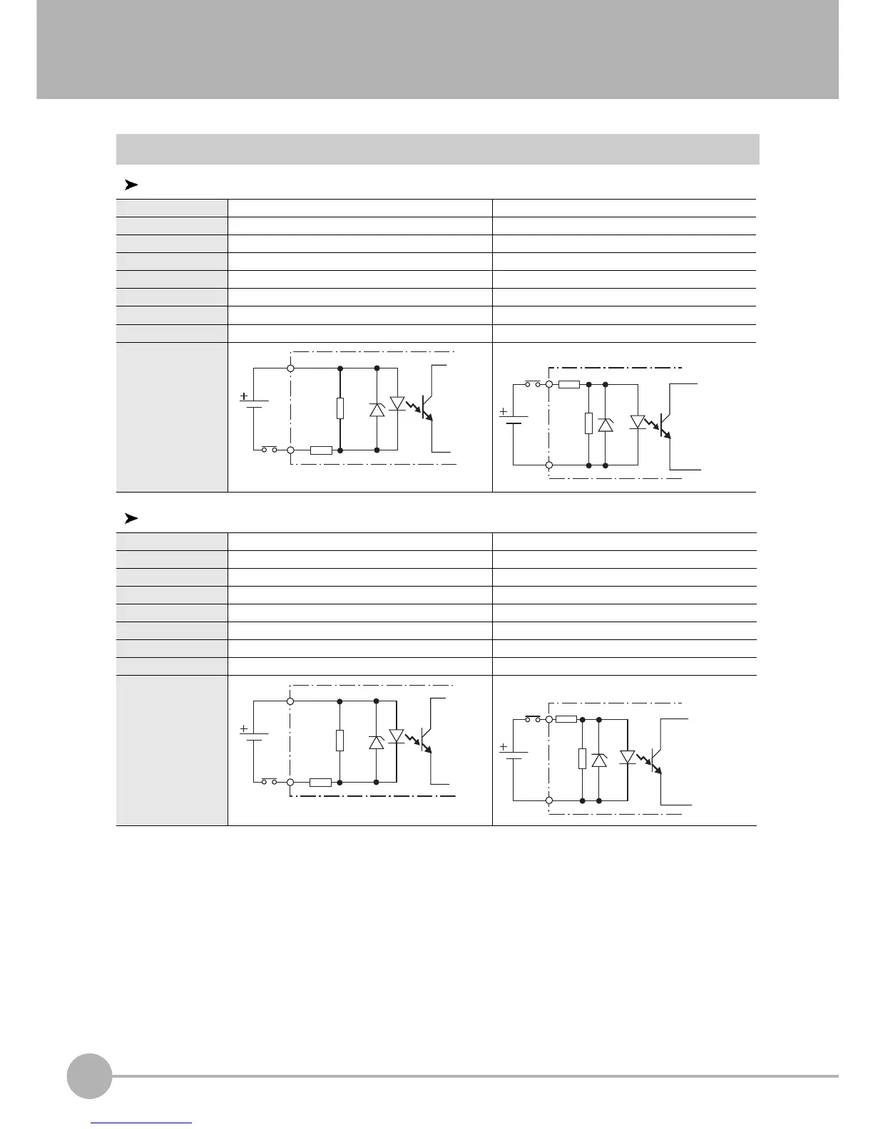
Input Specifications
RESET, DI0 to DI8, and DSA signals
TRIG signal
*1: The ON current/voltage is the value of the current/voltage that changes the status from OFF to ON. The
value of the ON voltage is the potential difference between COM IN and each input terminal.
*2: The OFF current/voltage is the value of the current/voltage that changes the status from ON to OFF. The
value of the OFF voltage is the potential difference between COM IN and each input terminal.
*3: The ON/OFF delay time for TRIG signal is different from the circuit diagram for RESET, DI0 to DI8, and DSA signals.
Mode NPN PNP
Input voltage 12 to 24 VDC ±10% 12 to 24 VDC ±10%
ON current *1 5 mA min. 5 mA min.
ON voltage *1 8.8 V min. 8.8 V min.
OFF current *2 0.5 mA max. 0.5 mA max.
OFF voltage *2 1.1 V max. 1.1 V max.
ON delay 5 ms max. 5 ms max.
OFF delay 0.7 ms max. 0.7 ms max.
Internal circuit
diagram
Mode NPN PNP
Input voltage 12 to 24 VDC ±10% 12 to 24 VDC ±10%
ON current *1 5 mA min. 5 mA min.
ON voltage *1 8.8 V min. 8.8 V min.
OFF current *2 0.5 mA max. 0.5 mA max.
OFF voltage *2 0.8 V max. 0.8 V max.
ON delay 0.1 ms max. 0.1 ms max.
OFF delay 0.1 ms max. 0.1 ms max.
Internal circuit
diagram
COMIN
Respective
terminal