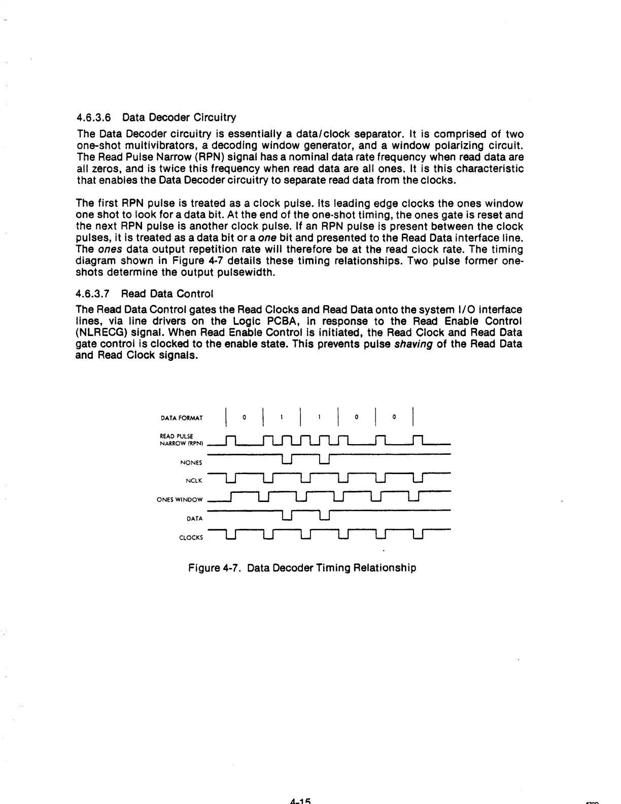
4.6.3.6 Data Decoder Circuitry
The
Data Decoder circuitry is essentially a data/clock separator. It is comprised of two
one-shot multivibrators, a decoding window generator, and a window polarizing circuit.
The
Read
Pulse Narrow
(RPN)
signal has a nominal data rate frequency when
read
data are
all zeros,
and
is twice this frequency when
read
data are all ones. It is this characteristic
that enables the Data Decoder circuitry to separate
read
data from the clocks.
The first
RPN
pulse is treated
as
a clock pulse. Its leading edge clocks the ones window
one shot to look for a data bit. At the end of the
one·shot timing, the ones gate is reset and
the next
RPN
pulse is another clock pulse.
If
an
RPN
pulse is present between the clock
pulses,
it
is treated
as
a data bit or a one bit and presented to the
Read
Data interface line.
The
ones data output repetition rate will therefore
be
at the read clock rate. The timing
diagram shown in Figure
4-7
details these timing relationships. Two pulse former one·
shots determine the output pulsewidth.
4.6.3.7
Read
Data Control
The
Read
Data Control gates the
Read
Clocks and
Read
Data onto the system
1/0
interface
lines, via
line drivers on the Logic PCBA, in response to the
Read
Enable Control
(NLRECG) signal.
When
Read
Enable Control Is initiated, the
Read
Clock and
Read
Data
gate control is clocked
to
the enable state. This prevents pulse shaving
of
the
Read
Data
and
Read
Clock signals.
DATA
FORMAT
READ
PULSE
NARROW
(RPN)
NONES
NCLK
ONES WINDOW
DATA
CLOCKS
o
o
o
Figure 4-7. Data Decoder Timing Relationship
A..1~