Sun Microelectronics
341
E. Pin and Signal Descriptions
E.2.6 IEEE 1149.1 (JTAG) Interface Pins
E.2.7 Initialization Interface Pins
E.3 Signal Descriptions
E.3.1 UltraSPARC Signals
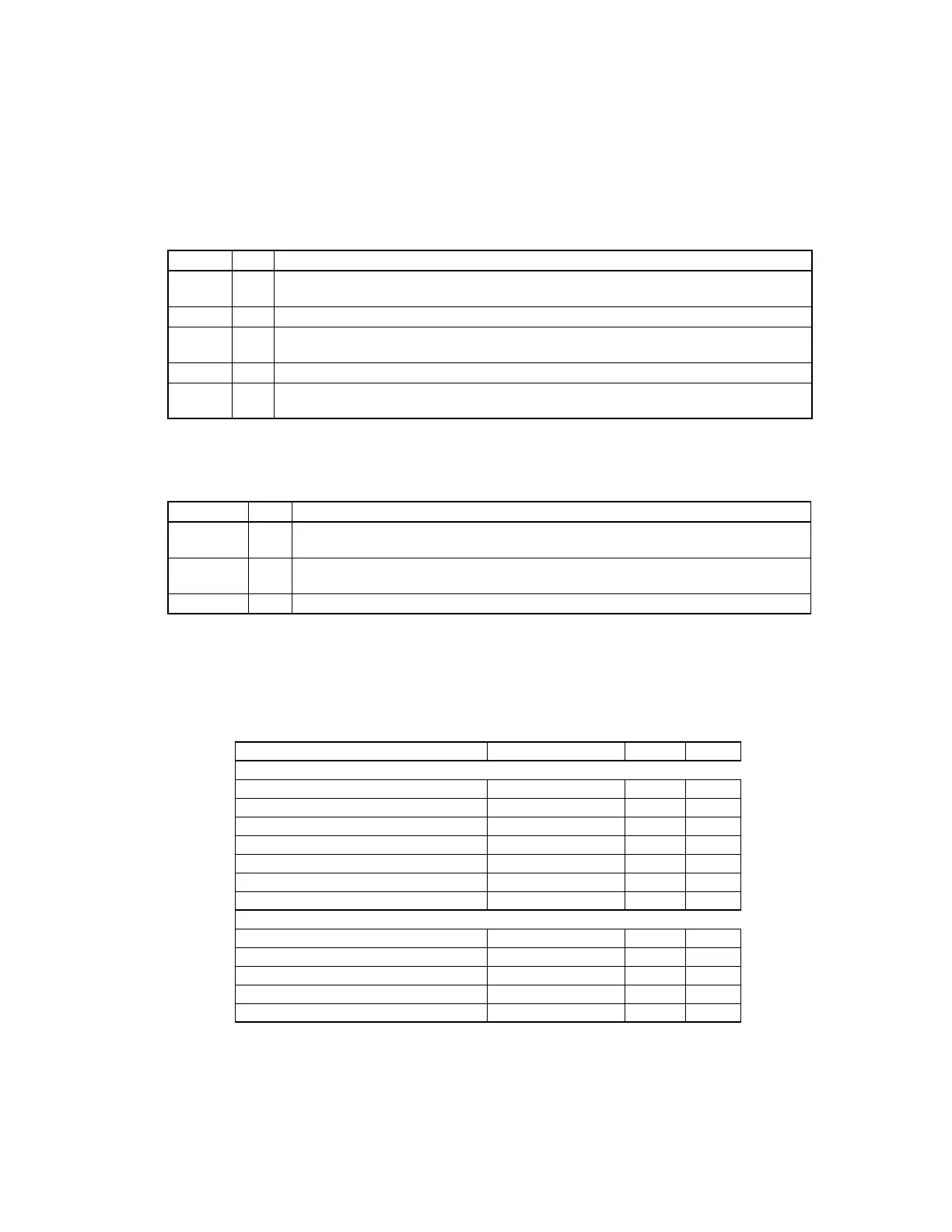
Table E-6 IEEE 1149.1 (JTAG) Interface Pins
Symbol Type Name and Function
TDO O IEEE 1149.1 test data output. A three-state signal driven only when the Test Access Port (TAP)
controller is in the shift-DR state.
TDI I IEEE 1149.1 test data input.
TCK I IEEE 1149.1 test clock input. If this pin is not connected to a clock source then TRST_L must be
asserted during POR.
TMS I IEEE 1149.1 test mode select input. This pin should externally be pulled high when not driven.
TRST_L I IEEE 1149.1 test reset input (active low). This pin should externally be pulled high when not
driven.
Table E-7 Initialization Interface Pins
Symbol Type Name and Function
RESET_L I Asserted asynchronously for POR (power-on) resets. Deasserted synchronous to system
clock. Active low.
XIR_L I Asserted to signal XIR resets. Acts like an edge triggered non-maskable interrupt. Synchro-
nous to system clock. Active low.
EPD O Asserted when UltraSPARC is in power-down mode.
Table E-8 UltraSPARC Signals
Function Name Count I/O
Data Transfer
E-Cache Data Bus EDATA<127:0> 128 I/O
E-Cache Data Bus Parity EDPAR<15:0> 16 I/O
E-Cache Data Address Bus ECAD<17:0>
1
18
1
O
E-Cache Tag Data Bus TDATA<24:0> 25 I/O
E-Cache Tag Data Parity TPAR<3:0> 4 I/O
E-Cache Tag Address Bus ECAT<15:0>
2
16
2
O
System Address Bus SYSADDR<36:0> 37 I/O
Data Transfer Controls
E-Cache Data Byte Write Enables BYTE_WE_L<15:0> 16 O
Data RAMs Write DSYN_WR_L 1 O
Data RAMs Output Enable DOE_L 1 O
Tag RAM Write TSYN_WR_L 1 O
Tag RAM Output Enable TOE_L 1 O
Artisan Technology Group - Quality Instrumentation ... Guaranteed | (888) 88-SOURCE | www.artisantg.com
 Loading...