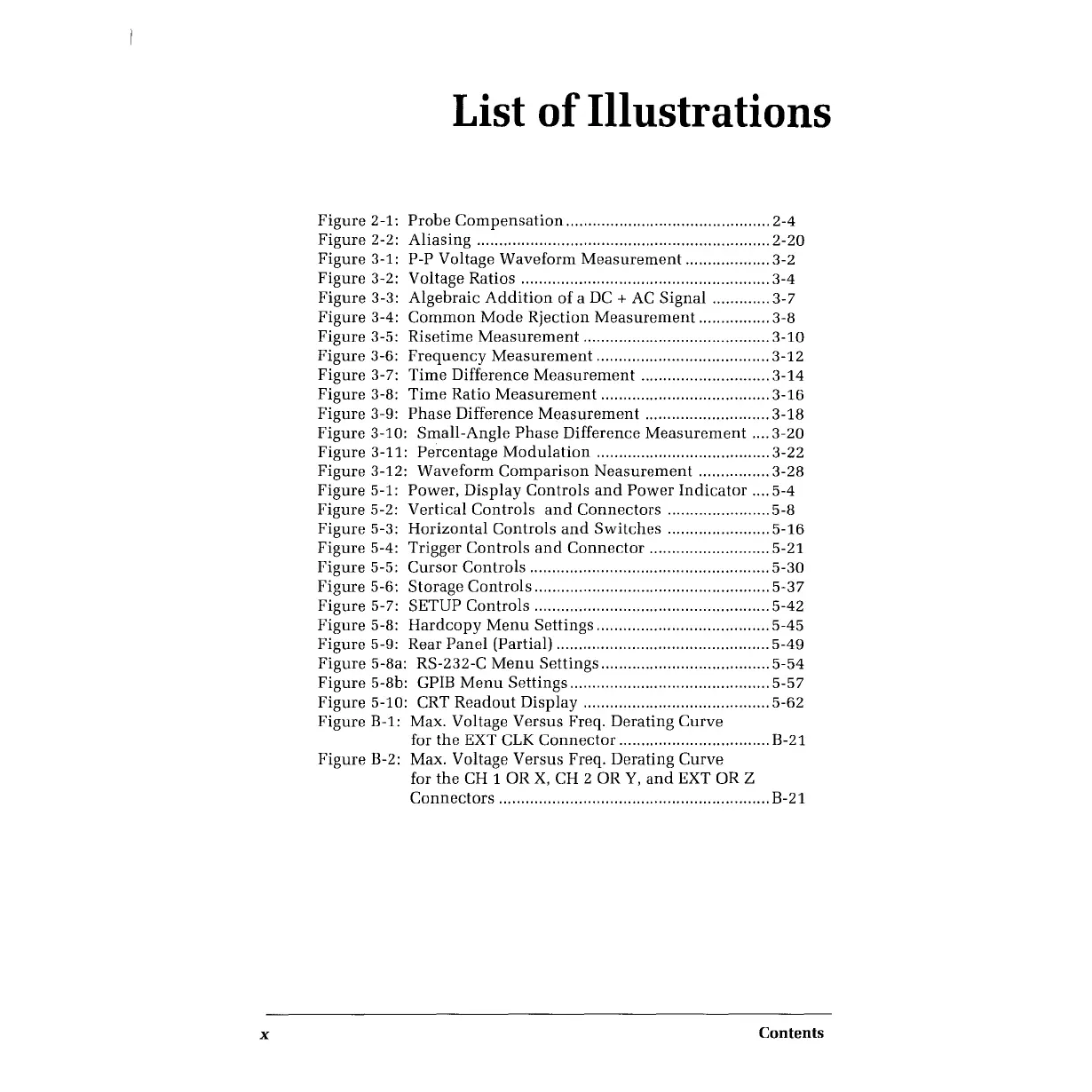
List
of
Illustrations
Figure
2-1:
Probe
Compensation
.............................................. 2-4
Figure
2-2:
Aliasing
.................................................................. 2-20
Figure
3-1: P-P Voltage
Waveform
Measurement
................... 3-2
Figure
3-2: Voltage Ratios ........................................................ 3-4
Figure
3-3:
Algebraic
Addition
of
a
DC+
AC
Signal
............. 3-7
Figure
3-4:
Common
Mode
Rjection
Measurement
................ 3-8
Figure
3-5:
Risetime
Measurement
.......................................... 3-10
Figure
3-6:
Frequency
Measurement
....................................... 3-12
Figure
3-7:
Time
Difference
Measurement
............................. 3-14
Figure
3-8:
Time
Ratio
Measurement
...................................... 3-16
Figure
3-9:
Phase
Difference
Measurement
............................ 3-18
Figure
3-10:
Small-Angle
Phase
Difference
Measurement
.... 3-20
Figure
3-11:
Percentage
Modulation
....................................... 3-22
Figure
3-12:
Waveform
Comparison
Neasurement
................ 3-28
Figure
5-1:
Power,
Display
Controls
and
Power
Indicator
.... 5-4
Figure
5-2:
Vertical
Controls
and
Connectors
....................... 5-8
Figure
5-3:
Horizontal
Controls
and
Switches
....................... 5-16
Figure
5-4: Trigger
Controls
and
Connector
........................... 5-21
Figure
5-5:
Cursor
Controls
...................................................... 5-30
Figure
5-6:
Storage
Controls
..................................................... 5-37
Figure
5-7: SETUP
Controls
..................................................... 5-42
Figure
5-8:
Hardcopy
Menu
Settings
....................................... 5-45
Figure
5-9:
Rear
Panel
(Partial) ................................................ 5-49
Figure
5-8a: RS-232-C
Menu
Settings
...................................... 5-54
Figure
5-8b: GPIB
Menu
Settings
............................................. 5-5 7
Figure
5-10: CRT
Readout
Display
.......................................... 5-62
Figure
B-1: Max. Voltage
Versus
Freq.
Derating
Curve
for
the
EXT CLK
Connector
.................................. B-21
Figure
B-2: Max. Voltage
Versus
Freq.
Derating
Curve
for
the
CH 1 OR
X,
CH 2
ORY,
and
EXT OR Z
Connectors
............................................................. B-21
X
Contents
 Loading...