MicroBlaze Processor Reference Guide 43
UG984 (v2018.2) June 21, 2018 www.xilinx.com
Chapter 2: MicroBlaze Architecture
With extended data addressing is enabled (parameter C_ADDR_SIZE > 32), the 32 least
significant bits of PVR8 and PVR9 are read with the MFS instruction, and the most
significant bits with the MFSE instruction.
When physical address extension (PAE) is enabled (parameters C_USE_MMU = 3 and
C_ADDR_SIZE > 32), the 32 least significant bits of PVR6 and PVR7 are read with the MFS
instruction, and the most significant bits with the MFSE instruction.
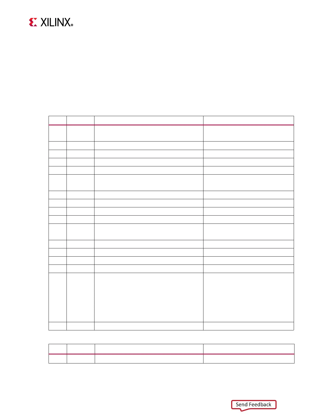
Table 2-24 through Table 2-36 provide bit descriptions and values.
Table 2-24: Processor Version Register 0 (PVR0)
Bits Name Description Value
0 CFG PVR implementation:
0 = Basic, 1 = Full
Based on C_PVR
1 BS Use barrel shifter
C_USE_BARREL
2 DIV Use divider C_USE_DIV
3 MUL Use hardware multiplier C_USE_HW_MUL > 0 (None)
4 FPU Use FPU C_USE_FPU > 0 (None)
5 EXC Use any type of exceptions Based on C_*_EXCEPTION
Also set if C_USE_MMU > 0 (None)
6 ICU Use instruction cache C_USE_ICACHE
7 DCU Use data cache C_USE_DCACHE
8 MMU Use MMU C_USE_MMU > 0 (None)
9 BTC Use branch target cache C_USE_BRANCH_TARGET_CACHE
10 ENDI Selected endianness:
Always 1 = Little endian
C_ENDIANNESS
11 FT Implement fault tolerant features C_FAULT_TOLERANT
12 SPROT Use stack protection C_USE_STACK_PROTECTION
13 REORD Implement reorder instructions C_USE_REORDER_INSTR
14:15 Reserved 0
16:23 MBV MicroBlaze release version code Release Specific
0x19 = v8.40.b
0x1B = v9.0
0x1D = v9.1
0x1F = v9.2
0x20 = v9.3
0x21 = v9.4
0x22 = v9.5
0x23 = v9.6
0x24 = v10.0
24:31 USR1 User configured value 1 C_PVR_USER1
Table 2-25: Processor Version Register 1 (PVR1)
Bits Name Description Value
0:31 USR2 User configured value 2 C_PVR_USER2