104
7647H–AVR–03/12
Atmel ATmega16/32/64/M1/C1
12.8.2 Timer/Counter Control Register B – TCCR0B
• Bit 7 – FOC0A: Force Output Compare A
The FOC0A bit is only active when the WGM bits specify a non-PWM mode.
However, for ensuring compatibility with future devices, this bit must be set to zero when
TCCR0B is written when operating in PWM mode. When writing a logical one to the FOC0A bit,
an immediate Compare Match is forced on the Waveform Generation unit. The OC0A output is
changed according to its COM0A1:0 bits setting. Note that the FOC0A bit is implemented as a
strobe. Therefore it is the value present in the COM0A1:0 bits that determines the effect of the
forced compare.
A FOC0A strobe will not generate any interrupt, nor will it clear the timer in CTC mode using
OCR0A as TOP.
The FOC0A bit is always read as zero.
• Bit 6 – FOC0B: Force Output Compare B
The FOC0B bit is only active when the WGM bits specify a non-PWM mode.
However, for ensuring compatibility with future devices, this bit must be set to zero when
TCCR0B is written when operating in PWM mode. When writing a logical one to the FOC0B bit,
an immediate Compare Match is forced on the Waveform Generation unit. The OC0B output is
changed according to its COM0B1:0 bits setting. Note that the FOC0B bit is implemented as a
strobe. Therefore it is the value present in the COM0B1:0 bits that determines the effect of the
forced compare.
A FOC0B strobe will not generate any interrupt, nor will it clear the timer in CTC mode using
OCR0B as TOP.
The FOC0B bit is always read as zero.
• Bits 5:4 – Res: Reserved Bits
These bits are reserved bits in the ATmega16/32/64/M1/C1 and will always read as zero.
• Bit 3 – WGM02: Waveform Generation Mode
See the description in the “Timer/Counter Control Register A – TCCR0A” on page 101.
• Bits 2:0 – CS02:0: Clock Select
The three Clock Select bits select the clock source to be used by the Timer/Counter.
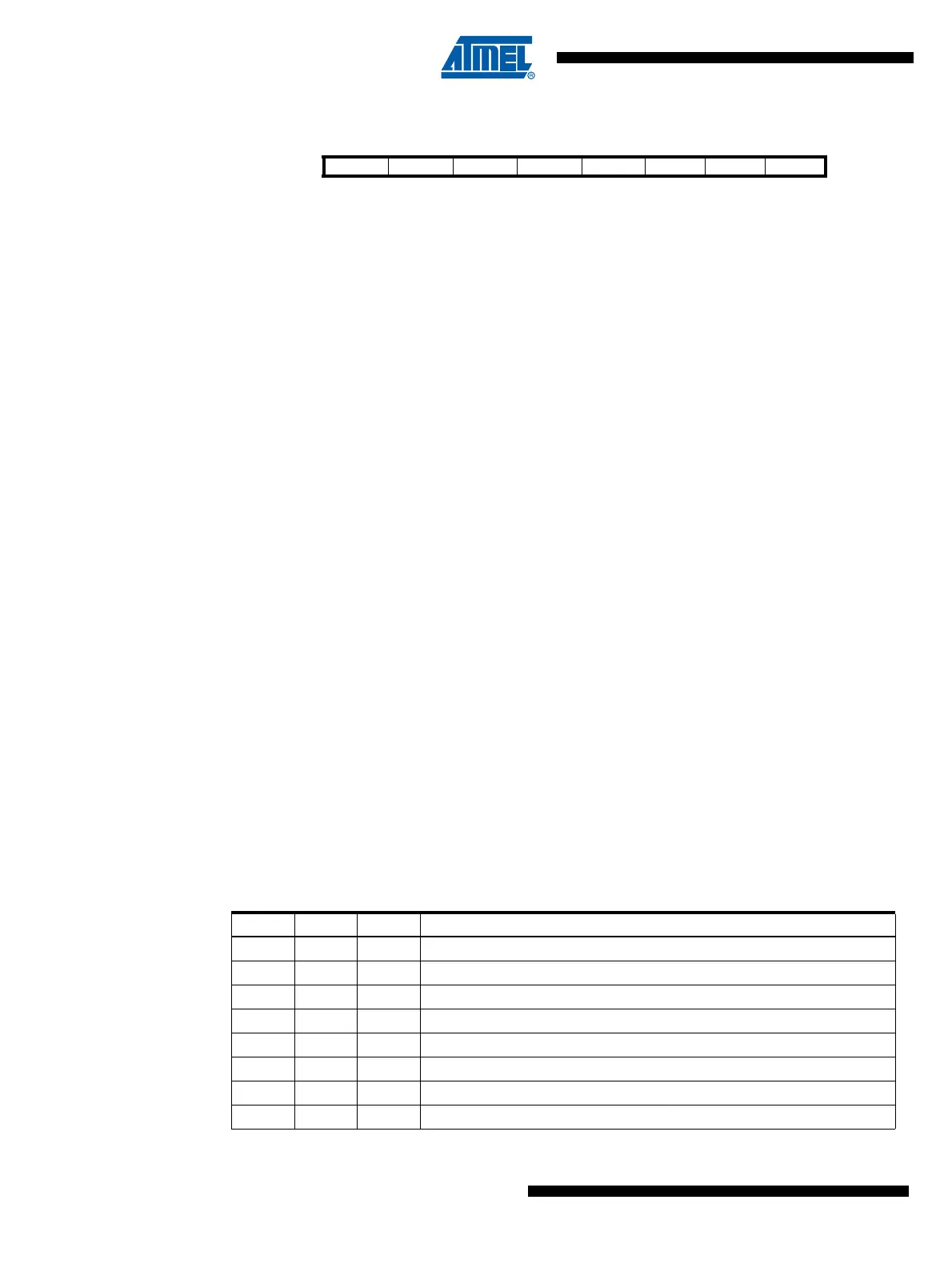
Bit 7 6 5 4 3 2 1 0
FOC0A FOC0B – – WGM02 CS02 CS01 CS00 TCCR0B
Read/Write W W R R R/W R/W R/W R/W
Initial Value 0 0 0 0 0 0 0 0
Table 12-9. Clock Select Bit Description
CS02 CS01 CS00 Description
0 0 0 No clock source (Timer/Counter stopped)
001clk
I/O
/(No prescaling)
010clk
I/O
/8 (From prescaler)
011clk
I/O
/64 (From prescaler)
100clk
I/O
/256 (From prescaler)
101clk
I/O
/1024 (From prescaler)
1 1 0 External clock source on T0 pin. Clock on falling edge.
1 1 1 External clock source on T0 pin. Clock on rising edge.