306
7647H–AVR–03/12
Atmel ATmega16/32/64/M1/C1
F. Repeat B through E until the entire buffer is filled or until all data within the page is loaded.
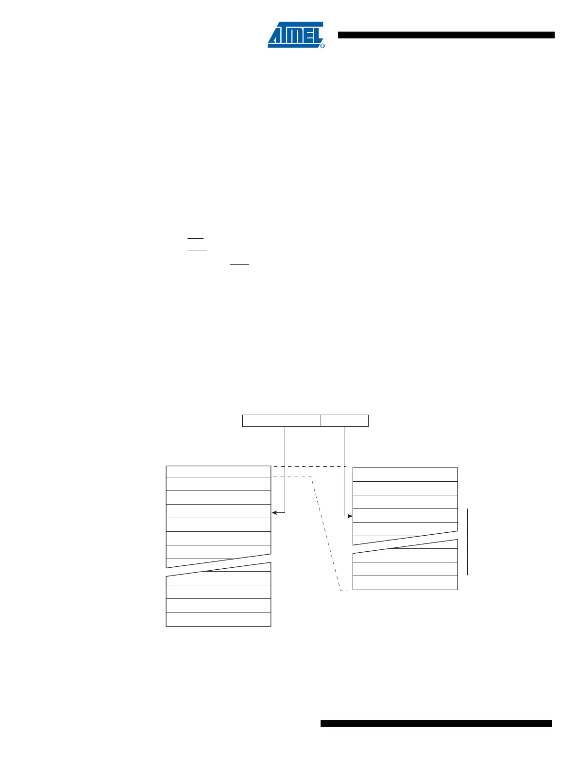
While the lower bits in the address are mapped to words within the page, the higher bits address
the pages within the FLASH. This is illustrated in Figure 25-2 on page 306. Note that if less than
eight bits are required to address words in the page (pagesize < 256), the most significant bit(s)
in the address low byte are used to address the page when performing a Page Write.
G. Load Address High byte
1. Set XA1, XA0 to “00”. This enables address loading.
2. Set BS1 to “1”. This selects high address.
3. Set DATA = Address high byte (0x00 - 0xFF).
4. Give XTAL1 a positive pulse. This loads the address high byte.
H. Program Page
1. Give WR
a negative pulse. This starts programming of the entire page of data.
RDY/BSY
goes low.
2. Wait until RDY/BSY
goes high (See Figure 25-3 for signal waveforms).
I. Repeat B through H until the entire Flash is programmed or until all data has been
programmed.
J. End Page Programming
1. 1. Set XA1, XA0 to “10”. This enables command loading.
2. Set DATA to “0000 0000”. This is the command for No Operation.
3. Give XTAL1 a positive pulse. This loads the command, and the internal write signals
are reset.
Figure 25-2. Addressing the Flash Which is Organized in Pages
(1)
Note: 1. PCPAGE and PCWORD are listed in Table 25-12 on page 303.
PROGRAM MEMORY
WORD ADDRESS
WITHIN A PAGE
PAGE ADDRESS
WITHIN THE FLASH
INSTRUCTION WORD
PAGE
PCWORD[PAGEMSB:0]:
00
01
02
PAGEEND
PAGE
PCWORDPCPAGE
PCMSB
PAGEMSB
PROGRAM
COUNTER