307
7647H–AVR–03/12
Atmel ATmega16/32/64/M1/C1
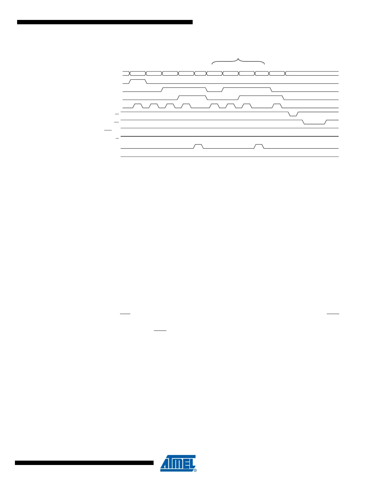
Figure 25-3. Programming the Flash Waveforms
(1)
Note: 1. “XX” is don’t care. The letters refer to the programming description above.
25.8.5 Programming the EEPROM
The EEPROM is organized in pages, see Table 25-13 on page 303. When programming the
EEPROM, the program data is latched into a page buffer. This allows one page of data to be
programmed simultaneously. The programming algorithm for the EEPROM data memory is as
follows (refer to “Programming the Flash” on page 305 for details on Command, Address and
Data loading):
1. A: Load Command “0001 0001”.
2. G: Load Address High Byte (0x00 - 0xFF).
3. B: Load Address Low Byte (0x00 - 0xFF).
4. C: Load Data (0x00 - 0xFF).
5. E: Latch data (give PAGEL a positive pulse).
K: Repeat 3 through 5 until the entire buffer is filled.
L: Program EEPROM page
1. Set BS1 to “0”.
2. Give WR
a negative pulse. This starts programming of the EEPROM page. RDY/BSY
goes low.
3. Wait until to RDY/BSY
goes high before programming the next page (See Figure 25-4
for signal waveforms).
RDY/BSY
WR
OE
RESET +12V
PAGEL
BS2
0x10 ADDR. LOW
ADDR. HIGH
DATA
DATA L OW DATA H I GH ADDR. LOW DATA LOW DATA HIGH
XA1
XA0
BS1
XTAL1
XX XX
XX
ABCDEBCDEGH
F