FIMER_PVS-175-TL A.1 Version_Product manual_EN_RevC-
F
41
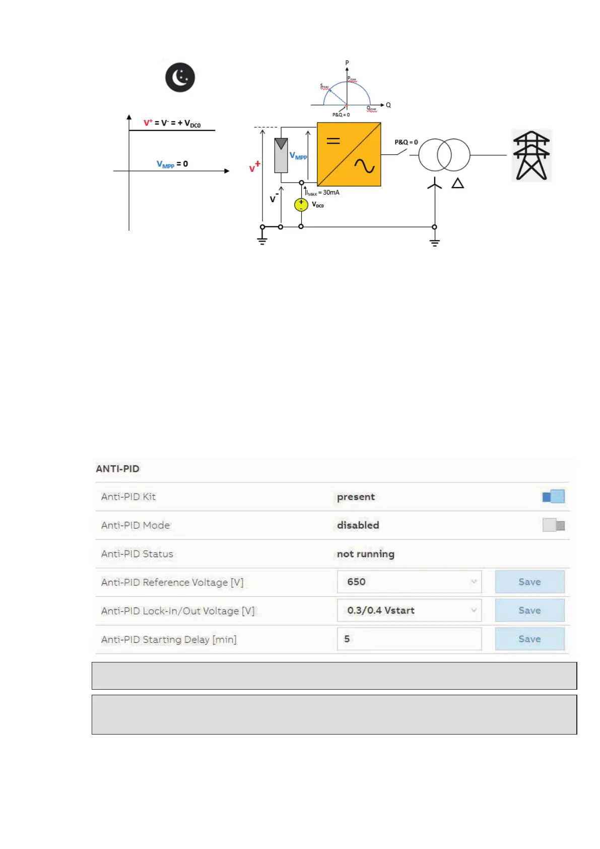
In the figure PVS-175’s array terminal voltages with respect to ground during night-time operation of the Anti-
PID board, inverter is off-line
Adjustable functions:
1) Output voltage, based on 3 pre-defined values: 500Vdc, 650Vdc (default), 800 Vdc
2) Activation and de-activation voltage
the Anti-PID function starts operating when input open circuit voltage VOC drops below selected activation
voltage, while it stops operating when VOC rise above selected De-activation voltage.
The activation and de-activation voltage can be regulated in steps of 0.1*Vstart as follows:
ACTIVATION/DE-ACTIVATION Voltage:
• 0.1/0.2*Vstart;
• 0.2/0.3*Vstart;
• 0.3/0.4*Vstart; (default setting)
• 0.4/0.5*Vstart.
3) Activation time-out (default = 5min): the Anti-PID operation is activated when the input open circuit voltage
VOC drops below 0.3*Vstart for at least 5 minutes continuously, while de-activation is triggered
immediately when input open circuit voltage VOC exceeds 0.4*Vstart.
ATTENTION – A The DC switches must not be operated when Anti-PID is operating. When Anti-PID
is ON it is clearly identified by simultaneous blinking of green and yellow led.
WARNING – B When Anti-PID board is installed, before any intervention on the DC side, disconnect
the AC grid and refer to “Inverter total de-energization and safe access” paragraph on this manual to
know all the necessary steps to safely operate on the inverter.
DC link precharge board
DC Link precharge circuit function is provided as an additional function only for dedicated inverter models.