Installation Manual
Quidway S8500 Series Routing Switches List of Figures
Huawei Technologies Proprietary
List of Figures
Figure 1-1 Quidway S8505 ....................................................................................................1-1
Figure 1-2 Quidway S8508 ....................................................................................................1-2
Figure 1-3 Quidway S8512 ....................................................................................................1-2
Figure 1-4 S8505 slots...........................................................................................................1-3
Figure 1-5 S8508 slots...........................................................................................................1-4
Figure 1-6 S8512 slots...........................................................................................................1-5
Figure 1-7 Three-input PoE power frame ..............................................................................1-8
Figure 1-8 Panel of the fan tray for the S8500 series............................................................1-9
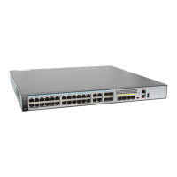
Figure 1-9 SRP1N0 panel.................................................................................................... 1-11
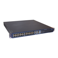
Figure 1-10 SRP1N1 panel..................................................................................................1-15
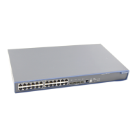
Figure 1-11 SRP1N2 panel..................................................................................................1-19
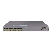
Figure 1-12 SRP1N3 panel..................................................................................................1-24
Figure 1-13 Front panel of the NAT service processor card................................................1-28
Figure 1-14 Rear panel of the NAT service processor card.................................................1-28
Figure 1-15 Front panel of the VPLS service processor card..............................................1-28
Figure 1-16 Rear panel of the VPLS service processor card ..............................................1-28
Figure 2-1 XP2 module panel ................................................................................................2-2
Figure 2-2 XP4 module panel ................................................................................................2-4
Figure 2-3 XK1 module panel ................................................................................................2-5
Figure 2-4 GT8P module panel..............................................................................................2-6
Figure 2-5 RJ-45 connector ...................................................................................................2-7
Figure 2-6 F32G module panel..............................................................................................2-9
Figure 2-7 RJ-45 connector .................................................................................................2-10
Figure 2-8 GP12 module panel............................................................................................ 2-11
Figure 2-9 GP24 module panel............................................................................................2-12
vi
 Loading...