Keysight Technologies N9040B UXA Signal Analyzer Service Guide 161
RF Section Troubleshooting (RF/Microwave Analyzers)
Troubleshooting
Troubleshooting a High Band Problem
Refer to the RF Highband Path #1 Block Diagram in Chapter 12 and follow the
instructions in the settings box. To enable the internal 4.8 GHz, −28 dBm
calibrator signal press Input/Output, RF Calibrator, 4.8 GHz.
A13 Front End Input Verification
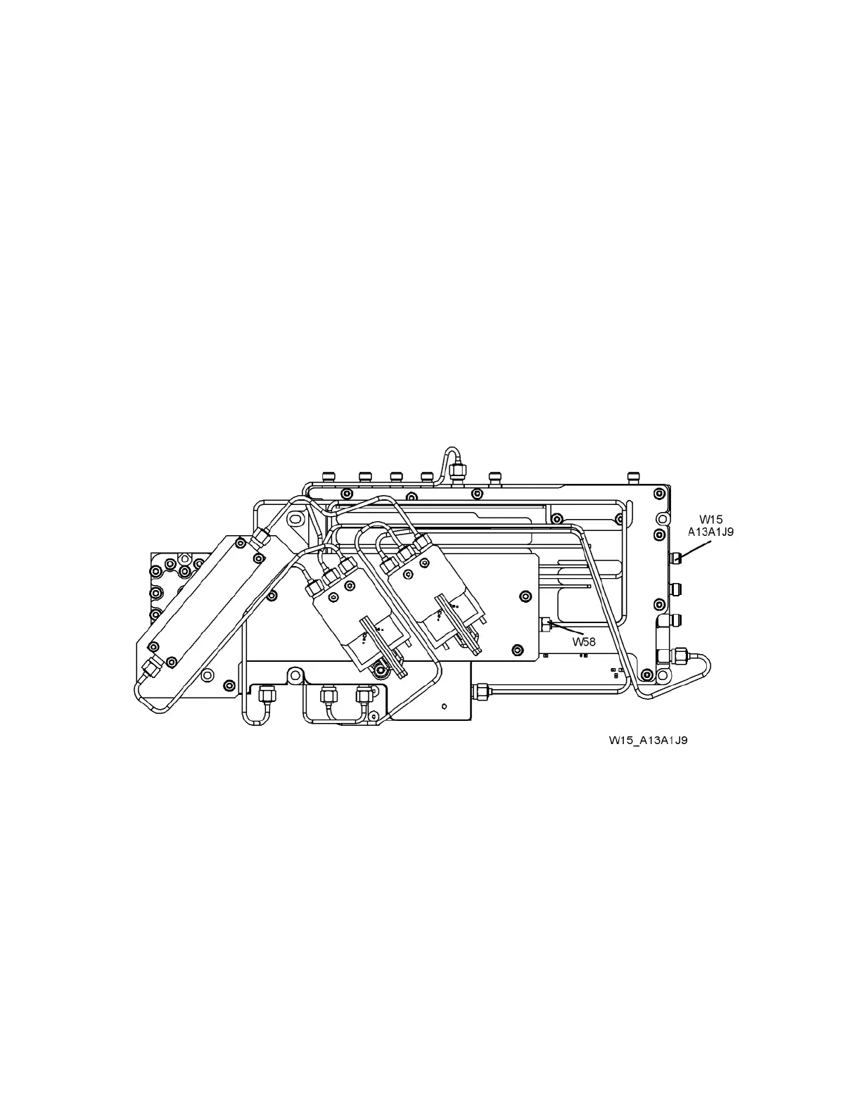
Disconnect W15 from A13A1J9 See Figure 4-10 for location of connector.
Loosen the other end of W15 which attaches to SW1to avoid damaging the
cable. Attach a right angle sma adapter to W15 and measure the input to the
A13 Front End with a spectrum analyzer.
Figure 4-10 A13A1J9 Location
Expected signal is 4.8 GHz at −51 dBm ± 4 dB. The tolerance is large because
the A12 YTF (microwave preselector) loss varies between devices, and the YTF
may not be perfectly aligned, or the frequency response adjustment may be
required.
If the signal level is incorrect, press AMPTD (Y Scale), Signal Path, uWPath
Control, uW Preselector Bypass. If the signal level is now −52 dBm, suspect
the A12 YTF is out of adjustment or faulty.
 Loading...