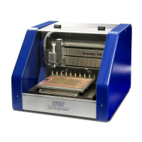
ProtoMat S Appendix
© 2011 LPKF AG HB V0.9/Mrz-11 97
10
Pos: 36 /ED_Technisc he_Dokumentation/2_Be dienungsanleitun g/Maschine/RP_Fräsb ohrplotter/Pr otoMat_S_Serie/Pr otoMat_S_Serie_II G/Kapitel_10_Anhang/ 10_2_Glossar @ 0\ mod_1255680492026_2058. docx @ 3968 @ 2
10.2 Glossary
B
Base copper Copper foil single or double sided fixed on the insulating
substrates for PCB.
Base material The isolated material applied with the copper circuit
structures (conductor tracks and annular rings). The base
material can be either inflexible or flexible (bendable).
D
Dielectric A dielectric is an electrically nonconductive, insulating
material.
Dispense A dispenser applies tiny amounts of the solder paste kept
in a cartridge on a printed circuit board.. The application of
SMD adhesive and other materials, which can be filled into
cartridges is called dispensing, too.
F
Fiducial Optical labelling on the surface of the printed circuit board
for correct arrangement. It is designates as OS as well.
L
Lamination A cathode-quality electrolytic copper deposition as a thin,
continuous sheet on rotating drums direct from refinery
electrolytes. Used as a conductor for printed circuits,
copper foil readily bonds to insulating substrates, accepts
the printed resists, and etches out to make printed circuits.
M
Multilayer A product consisting of alternate layers of conductive
patterns and insulating materials bonded together, with
conductive patterns in mote than two layers, and with the
conductive patterns interconnected as required.
P
Prepreg Prepregs are epoxy impregnated and pre-polymerised
glass cloth laminates for the construction of multilayer PCB.
Due to the good flow behaviour all clearances are filled up
free from air thus producing a perfect interpass fusion and
adhesion of the prepreg layers as well as the copper foils.
R
Resist Coating material used to mask or to protect selected areas
of a pattern from the action of an etchant solder, or plating
Rubout area Defined copper-free areas on the multilayer PCB will be
labelled as rubout area. Only the conductor tracks and the
annular rings are included.
S
Soldering stop
mask
Coatings which mask off and surface insulate those areas
of a circuit where soldering is not desired.
T
Throughplating An electrical connection between conductive patterns on
opposite sides of an insulating base, e.g. plated-through
hole or clinched jumper wire.