92
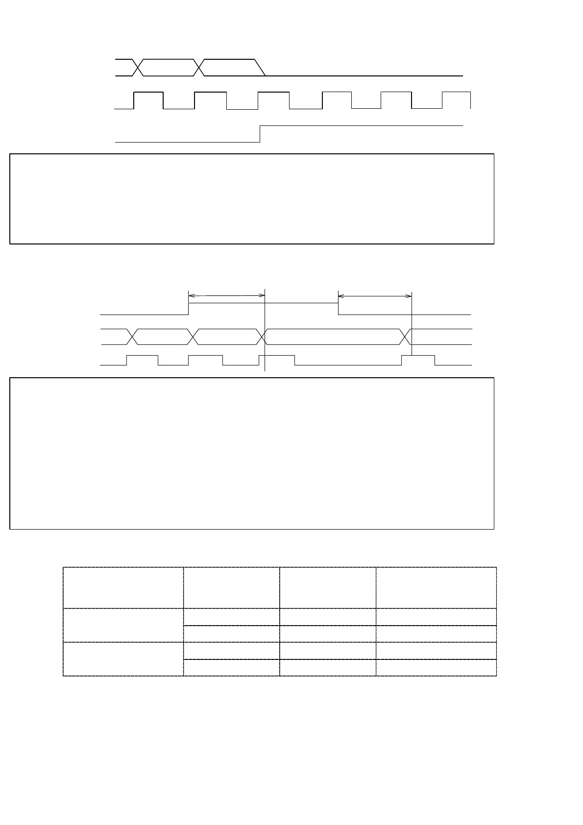
(3) When ERROR is occurred
DATA
POL.
P.C.
ON
ERROR
ON
ONON ON ONON
● At the time of ERROR output, output transistor at ERROR signal
will become ON(Negative logic electrically). Moreover, for each DATA,
POL., all of the output transistor will become OFF at the time of
ERROR output(Positive logic electrically).
(4) When the HOLD signal is input
DATA
POL
P.C.
HOLD
ON
4 times/s:Approx. 350 ms at max.
20 times/s:Approx. 150 ms at max.
4 times/s:Approx.350 ms at max.
20 times/s:Approx.150 ms at max.
● At the time of HOLD signal input, output transistor for the P.C. will
be OFF condition. (Positive logic electrically.)(However, for P.C.,OFF
condition will be made after one(1) shot of operation.)
● After inputting the HOLD signal, it takes the following response
times to freeze the DATA, POL or cancellation of HOLD is executed.
At the time of 20 times/s:Approx.150 ms at maximum
At the time of 4 times/s:Approx.350 ms at maximum
9−2−6. Output condition
Condition of
Pin−COM level
ett
ng output
og
c
u
pu
a
a
transistor
tt
et
me o
vo
tage
supply externally.
Yes ON L
egat
ve
og
c
No OFF H
Yes OFF H
os
t
ve
og
c
No ON L