Setting parameters
10/05 AWB8230-1541GB
70
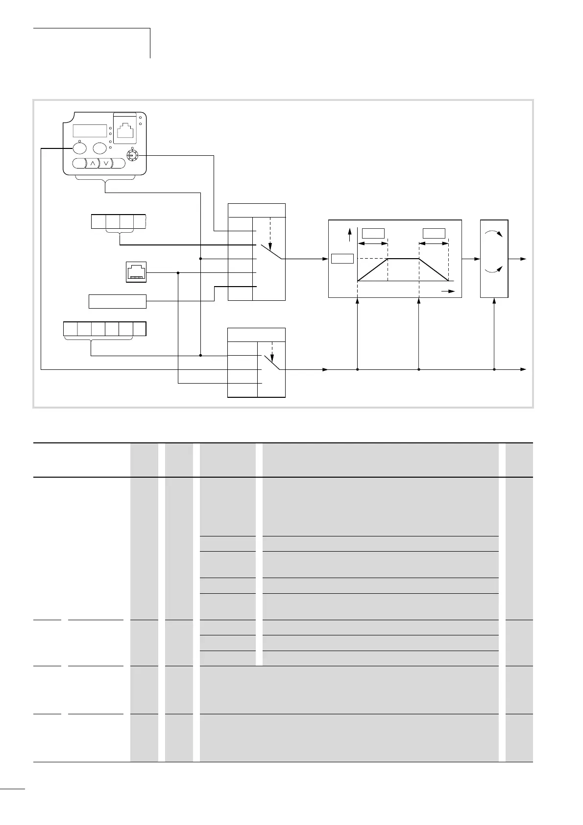
Figure 73: Block diagram, reference value/control signal input
PNU Name RUN b031
= 10
Value Function DS
A001 Reference
value source
selection
– – 00 The setting range is limited by PNU b082 (raised starting frequency) and
A004 (maximum frequency).
• Potentiometer (keypad)
•Frequency [Hz]
• Process variable [%] with active PID control (PNU A071 = 1)
01
01 Analog input: Control signal terminals O and OI
02 Set value (PNU F001) of the keypad (arrow keys Í/Ú). To save the set
value, press the ENTER key (PNU A020).
03 Serial interface (Modbus)
10 Calculator: Calculated value (CAL) (a section “Mathematical
functions”, page 127).
A002 Start signal
source
selection
– – 00 Digital input (FWD/REV) 01
01 LCD keypad: START and STOP key.
03 Modbus: Activates a COIL for RUN/STOP and a COIL for FWD/REV.
C081 Analog input O
– reference
value signal
compensation
j j Compensation of analog voltage signals at input O to output frequency (0 – 200 %) 100
C082 Analog input
OI – reference
value signal
compensation
j j Compensation of analog current signals at input OI to output frequency (0 – 200 %) 100
A
RUN
PRG
Hz
PRG
ENTER
IO
POWER
ALARM
OPE-Mode
00
01
02
03
10
H O OI L
F-COM
CAL
321P2454
A001
Modbus
01
02
03
A002
f
t
F001
0
F002
F003
STOP FWD/REVSTART
FWD
REV