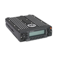
Chapter 8 Schematics, Boards Overlays, and Parts Lists
This chapter contains the schematics, board overlays, and parts lists
for the APX 7000/APX 7000XE radio. Use them in conjunction with
the theory of operation and the troubleshooting procedures, charts,
and waveforms to isolate a problem to the component level.
When schematics are viewed online or as a PDF file, colors can be
seen that denote power and signal paths. The red color denotes
voltage paths, blue denotes the receive path, and green denotes the
transmit path.
The following tables list the pages where the schematics and board
overlays for the APX 7000/APX 7000XE radio are found.
8.1 List of Transceiver Schematics and Board
Overlays
Table 8-1. Transceiver Schematics and Board Overlays
Transceiver Board Schematic/Board Layout
Page
No.
VHF / 700–800 MHz: MNUR4001B
MNUR4001B/D Transceiver (RF) Board Overall Circuit Schematic
8-4
MNUR4001B/D VHF Harmonic Filter Circuit 8-5
MNUR4001B/D 700–800 MHz Harmonic Filter Circuit 8-5
MNUR4001B GPS Circuit 8-6
MNUR4001B/D Miscellaneous Connector Circuit 8-8
MNUR4001B/D VHF Receiver Front End Circuit 8-9
MNUR4001B/D 700–800 MHz Receiver Front End Circuit 8-10
MNUR4001B Receiver Back End Circuit 8-11
MNUR4001B/D DC Power Circuit 8-13
MNUR4001B/D Transmitter and Automatic Level Control Circuits 8-14
MNUR4001B/D Frequency Generation Unit (Synthesizer) Circuit – 1 of 2 8-15
MNUR4001B/D Frequency Generation Unit (VCO) Circuit – 2 of 2 8-16
MNUR4001B/D Mixer and IF Filter Circuits 8-17
MNUR4001B/D VHF Power Amplifier Circuit 8-18
MNUR4001B/D 700–800 MHz Power Amplifier Circuit 8-19
MNUR4001B/D Transceiver (RF) Board Layout – Side 1 8-20
MNUR4001B/D Transceiver (RF) Board Layout – Side 2 8-21
UHF1 / 700–800: MNUS4000A/C/E
MNUS4000A/C/E Transceiver (RF) Board Overall Circuit Schematic
8-43
MNUS4000A//C/E UHF1 Harmonic Filter Circuit 8-44
MNUS4000A/C/E 700–800 MHz Harmonic Filter Circuit 8-44
MNUS4000A/C/E GPS Circuit 8-45
MNUS4000A/C/E Miscellaneous Connector Circuit 8-46
MNUS4000A//C/E UHF1 Receiver Front End Circuit 8-47
MNUS4000A/C/E 700–800 MHz Receiver Front End Circuit 8-48
MNUS4000A/C/E Receiver Back End Circuit 8-49
MNUS4000A/C/E DC Power Circuit 8-51
MNUS4000A/C/E Transmitter and Automatic Level Control Circuits 8-52
MNUS4000A/C/E Frequency Generation Unit (Synthesizer) Circuit – 1 of
2
8-53
MNUS4000A/C/E Frequency Generation Unit (VCO) Circuit – 2 of 2 8-54
MNUS4000A/C/E Mixer and IF Filter Circuits 8-55
MNUS4000A/E UHF1 Power Amplifier Circuit 8-56
MNUS4000C UHF1 Power Amplifier Circuit
8-57
MNUS4000A/C/E/F 700–800 MHz Power Amplifier Circuit 8-58
MNUS4000A/E Transceiver (RF) Board Layout – Side 1 8-59
MNUS4000A/E Transceiver (RF) Board Layout – Side 2 8-60
MNUS4000C/F Transceiver (RF) Board Layout – Side 1 8-61
MNUS4000C/F Transceiver (RF) Board Layout – Side 2 8-62
UHF1 / VHF: MNUT4000A/C/E
MNUT4000A/C/E Transceiver (RF) Board Overall Circuit Schematic
8-105
MNUT4000A/C/E UHF1 Harmonic Filter Circuit 8-106
MNUT4000A/C/E VHF MHz Harmonic Filter Circuit 8-106
Table 8-1. Transceiver Schematics and Board Overlays (Continued)
Transceiver Board Schematic/Board Layout
Page
No.
MNUT4000A/C/E GPS Circuit 8-107
MNUT4000A/C/E Miscellaneous Connector Circuit 8-108
MNUT4000A/C/E UHF1 Receiver Front End Circuit 8-109
MNUT4000A/C/E VHF Receiver Front End Circuit 8-110
MNUT4000A/C Receiver Back End Circuit 8-111
MNUT4000A/C/E DC Power Circuit 8-113
MNUT4000A/C/E Transmitter and Automatic Level Control Circuits 8-114
MNUT4000A/C/E Frequency Generation Unit (Synthesizer) Circuit – 1 of
2
8-115
MNUT4000A/C/E Frequency Generation Unit (VCO) Circuit – 2 of 2 8-116
MNUT4000A/C/E Mixer and IF Filter Circuits 8-117
MNUT4000A UHF1 Power Amplifier Circuit 8-118
MNUT4000C UHF1 Power Amplifier Circuit 8-119
MNUT4000A/C/E VHF Power Amplifier Circuit 8-120
MNUT4000A Transceiver (RF) Board Layout – Side 1 8-121
MNUT4000A Transceiver (RF) Board Layout – Side 2 8-122
MNUT4000C/E Transceiver (RF) Board Layout – Side 1 8-123
MNUT4000C/E Transceiver (RF) Board Layout – Side 2 8-124
UHF1 / UHF2: MNUE7367A
MNUE7367A Transceiver (RF) Board Overall Circuit Schematic
8-157
MNUE7367A UHF1 Harmonic Filter Circuit 8-158
MNUE7367A UHF2 MHz Harmonic Filter Circuit 8-158
MNUE7367A GPS Circuit 8-159
MNUE7367A Miscellaneous Connector Circuit 8-160
MNUE7367A UHF1 Receiver Front End Circuit 8-161
MNUE7367A UHF2 Receiver Front End Circuit 8-162
MNUE7367A Receiver Back End Circuit 8-163
MNUE7367A DC Power Circuit 8-165
Table 8-1. Transceiver Schematics and Board Overlays (Continued)
Transceiver Board Schematic/Board Layout
Page
No.
 Loading...