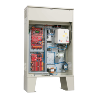
The Computer
5-42 Manual # 42-02-1P28 A3
LS-LSI Connector Assignments
Table 5.8 LS-LSI Connector Assignments
Connector Assignment Description
J1 SPD0 Speed bit 0 from the LS-EDGE landing system
J1 SPD1 Speed bit 1 from the LS-EDGE landing system
J1 DZF Front Door Zone signal from the LS-EDGE landing system
J1 24CTP 24VDC fused power out (F1 is 72V, 1100mA)
J2 CANH1 CAN port 1, H
J2 CANL1 CAN port 1, L
J2 CANH2 CAN port 2, H
J2 CANL2 CAN port 2, L
J2 SHLD CAN shield
J3, Pin 1 2 120VRMS from machine room
J3, Pin 2 1 Ground
J3, Pin 3 2 120VRMS to load weigher
J3, Pin 4 1 Ground
J4 24V 24V to first MC-CPI-2 board
J4 COM Common for 24V
J5 SPD0 Speed bit 0 from LS-EDGE sensor
J5 SPD1 Speed bit 1 from LS-EDGE sensor
J5 SPD2 Speed bit 2 from LS-EDGE sensor
J5 SP1A DTL
J5 SP2A DSL1
J5 SP3A USL1
J5 DZR M Door Zone Rear
J5 SP4A UTL
J5 CGND Pins 9 and 10. Chassis ground.
J6 CANH2 CAN port 2, H
J6 CANL2 CAN port 2, L
J6 DZF M Door Zone Front
J6 CANH1 CAN port 1, H
J6 12V BAT 12V, Battery output
J6 CANL1 CAN port 1, L
J6 DGND Ground
J6 V UNREG Unregulated ~24V
J6 CGND Pins 9 and 10. Chassis ground.
J7 SNN1 Unused
J7 V UNREG Unregulated ~24V from machine room
J7 CANH2 CAN port 2, H
J7 CANL2 CAN port 2, L
J7 Pins 4, 6 Ground
J7 M1, M2 Chassis ground
J8 SNN 2 Unused
J8 V UNREG Unregulated ~24V from machine room
J8 CANH2 CAN port 2, H
J8 CANL2 CAN port 2, L
J8 Pins 4, 6 Ground
J8 M1, M2 Chassis ground