Appendices
A-44
CJ2 CPU Unit Hardware User’s Manual
*1 The ON response time will be 20 µs maximum and OFF response time will be 400 µs maximum even if the response
times are set to 0 ms due to internal element delays.
Note Observe the following restrictions when connecting to a 2-wire sensor.
• Make sure the input power supply voltage does not exceed the ON voltage (19 V) plus the residual voltage of the
sensor (approx. 3 V).
• Use a sensor with a minimum load current of 3 mA min.
• Connect bleeder resistance if you connect a sensor with a minimum load current of 5 mA or higher.
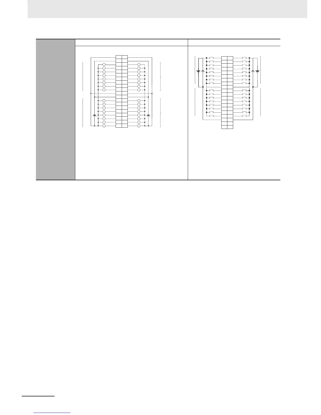
Terminal Connec-
tions
CN1 (OUT) CN2 (IN)
• Be sure to wire both terminals A19 and A9 (COM0 (0 V)) of
CN1.
• Be sure to wire both terminals B19 and B9 (COM1 (0 V)) of
CN1.
• Be sure to wire both terminals A20 and A10 (+V) of CN1.
• Be sure to wire both terminals B20 and B10 (+V) of CN1.
• When wiring, pay careful attention to the polarity of the exter-
nal power supply. The load may operate incorrectly if polarity
is reversed.
• Be sure to wire both pins A9 and A18 (COM2) of
CN2, and set the same polarity for both pins.
• Be sure to wire both pins B9 and B18 (COM3) of
CN2, and set the same polarity for both pins.
• When wiring, pay careful attention to the polarity
of the external power supply. The load may oper-
ate incorrectly if polarity is reversed.
A1
A2
A3
A4
A5
A6
A7
A8
OUT0
OUT1
OUT2
OUT3
OUT4
OUT5
OUT6
OUT7
A9
A10
A11
A12
A13
A14
A15
A16
A17
A18
OUT8
OUT9
OUT10
OUT11
OUT12
OUT13
OUT14
OUT15
A19
A20
B1
B2
B3
B4
B5
B6
B7
B8
OUT0
OUT1
OUT2
OUT3
OUT4
OUT5
OUT6
OUT7
B9
B10
+V
+V
B11
B12
B13
B14
B15
B16
B17
B18
OUT8
OUT9
OUT10
OUT11
OUT12
OUT13
OUT14
OUT15
B19
COM0 (0V) COM1 (0V)
B20
+V +V
L
L
L
L
L
L
L
L
L
L
L
L
L
L
L
L
L
L
L
L
L
L
L
L
L
L
L
L
L
L
L
L
COM0 (0V) COM1 (0V)
I/O word "m+1"
I/O word "m"
I/O word "m+1"
12 to
24
VDC
I/O word "m"
12 to
24
VDC
Signal
name
Signal
name
Connec-
tor pin
Allocated
CIO word
Allocated
CIO word
B1
IN0
B2
IN1
B3
IN2
B4
IN3
B5
IN4
B6
IN5
B7
IN6
B8
IN7
B9
B10
IN8
B11
IN9
B12
IN10
B13
IN11
B14
IN12
B15
IN13
B16
IN14
B17
IN15
B18
B19
NC
B20
NC
A1
IN0
A2
IN1
A3
IN2
A4
IN3
A5
IN4
A6
IN5
A7
IN6
A8
IN7
A9
A10
IN8
A11
IN9
A12
IN10
A13
IN11
A14
IN12
A15
IN13
A16
IN14
A17
IN15
COM2 COM3
COM2 COM3
A18
A19
NC
A20
NC
I/O word "m+2"
I/O word "m+3"
I/O word "m+2"
I/O word "m+3"
24
VDC
24
VDC
Signal
name
Signal
name
Connec-
tor pin
Allocated
CIO word
Allocated
CIO word