7-27
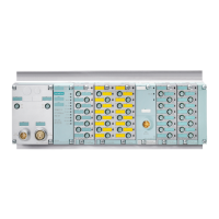
ET 200U Distributed I/O Station
EWA 4NEB 812 6087–02b
1
2
3579
46 810
L+ M
DC 24 V
QI
(4/8)
M
ANA
(6/10)
R
L
Key:
QI: Analog Output “Current”
M
ANA
: Chassis Ground Terminal of the Analog Unit
R
L
: Load Resistor
Figure 7-10Connection via a Two–Wire Circuit (6ES5 470–8MB11, 6ES5 470–8MC11)
Table 7-14 shows how the analog output value has to be stored in the process
image output table (PIQ).
Tables 7-15 and 7-16 show the voltage and currents assigned to the bit pat-
terns.
Table 7-14 Representation of an Analog Output Value as a Bit Pattern
High Byte Low Byte
Bit Number 7 6 5 4 3 2 1 0 7 6 5 4 3 2 1 0
Analog Value Represent. VZ 2
10
2
9
2
8
2
7
2
6
2
5
2
4
2
3
2
2
2
1
2
0
X X X X
X: Irrelevant bits
Analog Value Re-
presentation of
Analog Output Mo-
dules
Analog Value Processing
 Loading...