RM0440 Rev 4 143/2126
RM0440 Embedded Flash memory (FLASH) for category 3 devices
228
3.7.16 Flash Bank 2 WRP area B address register (FLASH_WRP2BR)
Address offset: 0x50
Reset value: 0x00XX 00XX
Access: no wait state when no Flash memory operation is on going, word, half-word and
byte access
3.7.17 Flash Securable area bank1 register (FLASH_SEC1R)
Address offset: 0x70
Reset value: 0xFFFX FFXX
Access: no wait state when no Flash memory operation is on going, word, half-word and
byte access
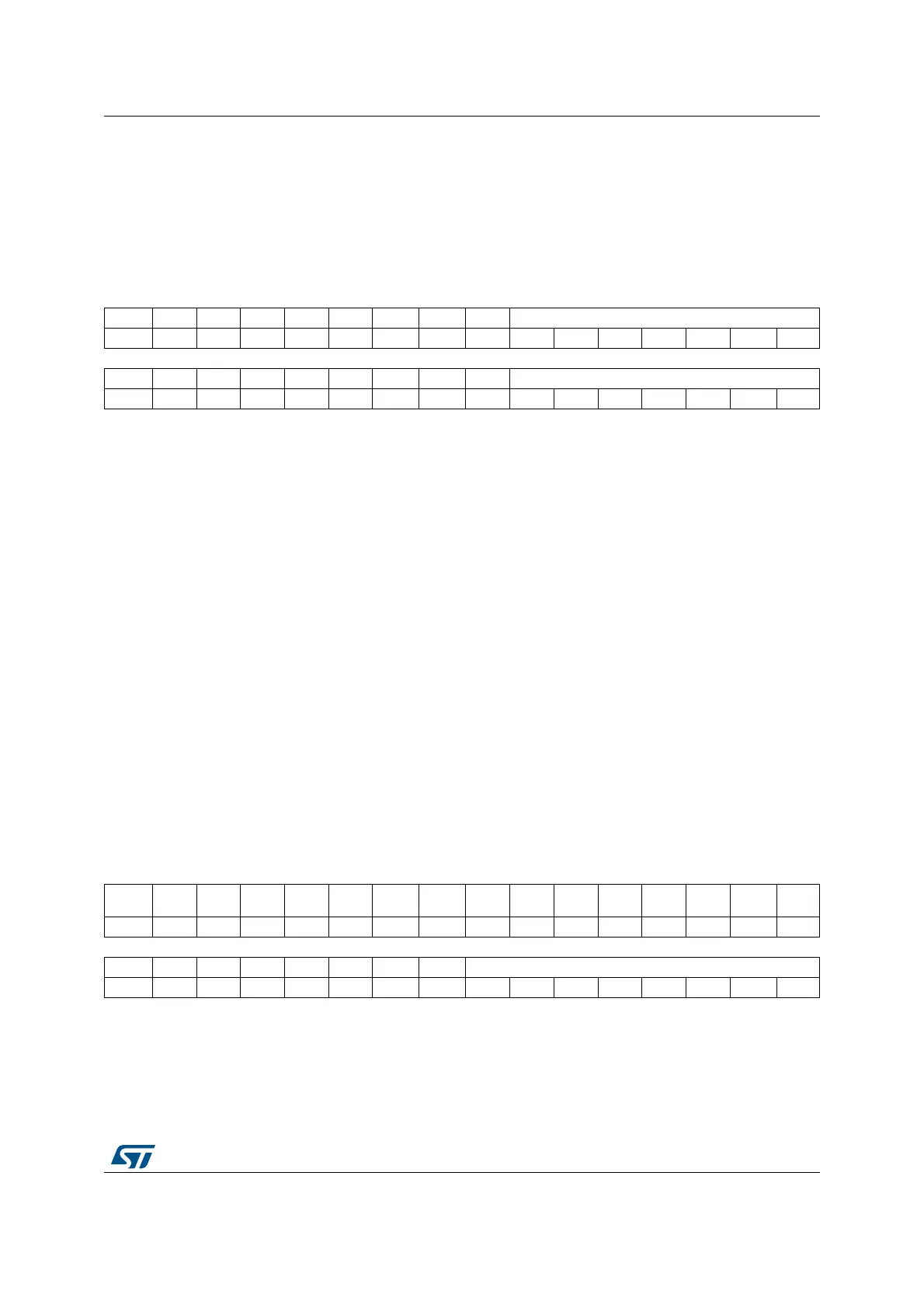
31 30 29 28 27 26 25 24 23 22 21 20 19 18 17 16
Res. Res. Res. Res. Res. Res. Res. Res. Res. WRP2B_END[7:0]
rw rw rw rw rw rw rw
15 14 13 12 11 10 9 8 7 6 5 4 3 2 1 0
Res. Res. Res. Res. Res. Res. Res. Res. Res. WRP2B_STRT[7:0]
rw rw rw rw rw rw rw
Bits 31:23 Reserved, must be kept cleared
Bits 22:16 WRP2B_END: WRP second area “B” end offset
DBANK=1
WRP2B_END contains the last page of the WRP second area for bank2.
DBANK=0
WRP2B_END contains the last page of the WRP fourth area for all memory.
Bits 15:7 Reserved, must be kept cleared
Bits 6:0 WRP2B_STRT: WRP second area “B” start offset
DBANK=1
WRP2B_STRT contains the first page of the WRP second area for bank2.
DBANK=0
WRP2B_STRT contains the first page of the WRP second area for all memory.
31 30 29 28 27 26 25 24 23 22 21 20 19 18 17 16
Res. Res. Res. Res. Res. Res. Res. Res. Res. Res. Res. Res. Res. Res. Res.
BOOT_
LOCK
rw
15 14 13 12 11 10 9 8 7 6 5 4 3 2 1 0
Res. Res. Res. Res. Res. Res. Res. Res. SEC_SIZE1
rw rw rw rw rw rw rw rw