Power control (PWR) RM0440
260/2126 RM0440 Rev 4
6.4.6 Power status register 2 (PWR_SR2)
Address offset: 0x14
Reset value: 0x0000 0000. This register is partially reset when exiting Standby/Shutdown
modes.
Bit 2 WUF3: Wakeup flag 3
This bit is set when a wakeup event is detected on wakeup pin, WKUP3. It is cleared by
writing ‘1’ in the CWUF3 bit of the PWR_SCR register.
Bit 1 WUF2: Wakeup flag 2
This bit is set when a wakeup event is detected on wakeup pin, WKUP2. It is cleared by
writing ‘1’ in the CWUF2 bit of the PWR_SCR register.
Bit 0 WUF1: Wakeup flag 1
This bit is set when a wakeup event is detected on wakeup pin, WKUP1. It is cleared by
writing ‘1’ in the CWUF1 bit of the PWR_SCR register.
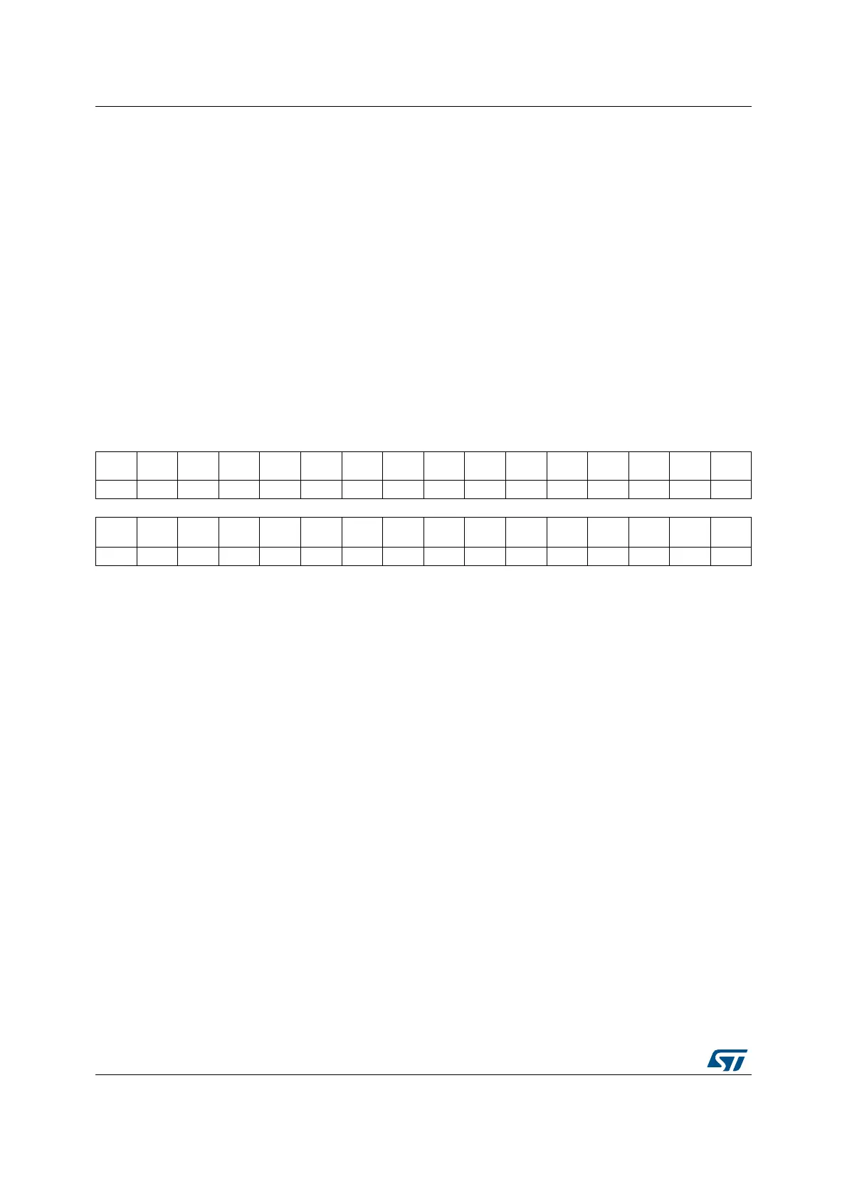
31 30 29 28 27 26 25 24 23 22 21 20 19 18 17 16
Res. Res. Res. Res. Res. Res. Res. Res. Res. Res. Res. Res. Res. Res. Res. Res.
1514131211109876543210
PVMO2 PVMO1 Res. Res. PVDO VOSF
REGLP
F
REGLP
S
Res. Res. Res. Res. Res. Res. Res. Res.
rr rrrr
Bits 31:16 Reserved, must be kept at reset value.
Bit 15 PVMO2: Peripheral voltage monitoring output: V
DDA
vs. 1.8 V
0: V
DDA
voltage is above PVM2 threshold (around 1.8 V).
1: V
DDA
voltage is below PVM2 threshold (around 1.8 V).
Note: PVMO2 is cleared when PVM2 is disabled (PVME = 0). After enabling PVM2, the PVM2
output is valid after the PVM2 wakeup time.
Bit 14 PVMO1: Peripheral voltage monitoring output: V
DDA
vs. 1.62 V
0: V
DDA
voltage is above PVM1 threshold (around 1.62 V).
1: V
DDA
voltage is below PVM1 threshold (around 1.62 V).
Note: PVMO1 is cleared when PVM1 is disabled (PVME = 0). After enabling PVM1, the PVM1
output is valid after the PVM1 wakeup time.
Bits 13:12 Reserved, must be kept at reset value.
Bit 11 PVDO: Programmable voltage detector output
0: V
DD
is above the selected PVD threshold
1: V
DD
is below the selected PVD threshold
Bit 10 VOSF: Voltage scaling flag
A delay is required for the internal regulator to be ready after the voltage scaling has been
changed. VOSF indicates that the regulator reached the voltage level defined with VOS bits
of the PWR_CR1 register.
0: The regulator is ready in the selected voltage range
1: The regulator output voltage is changing to the required voltage level