RM0440 Rev 4 1347/2126
RM0440 General-purpose timers (TIM15/TIM16/TIM17)
1445
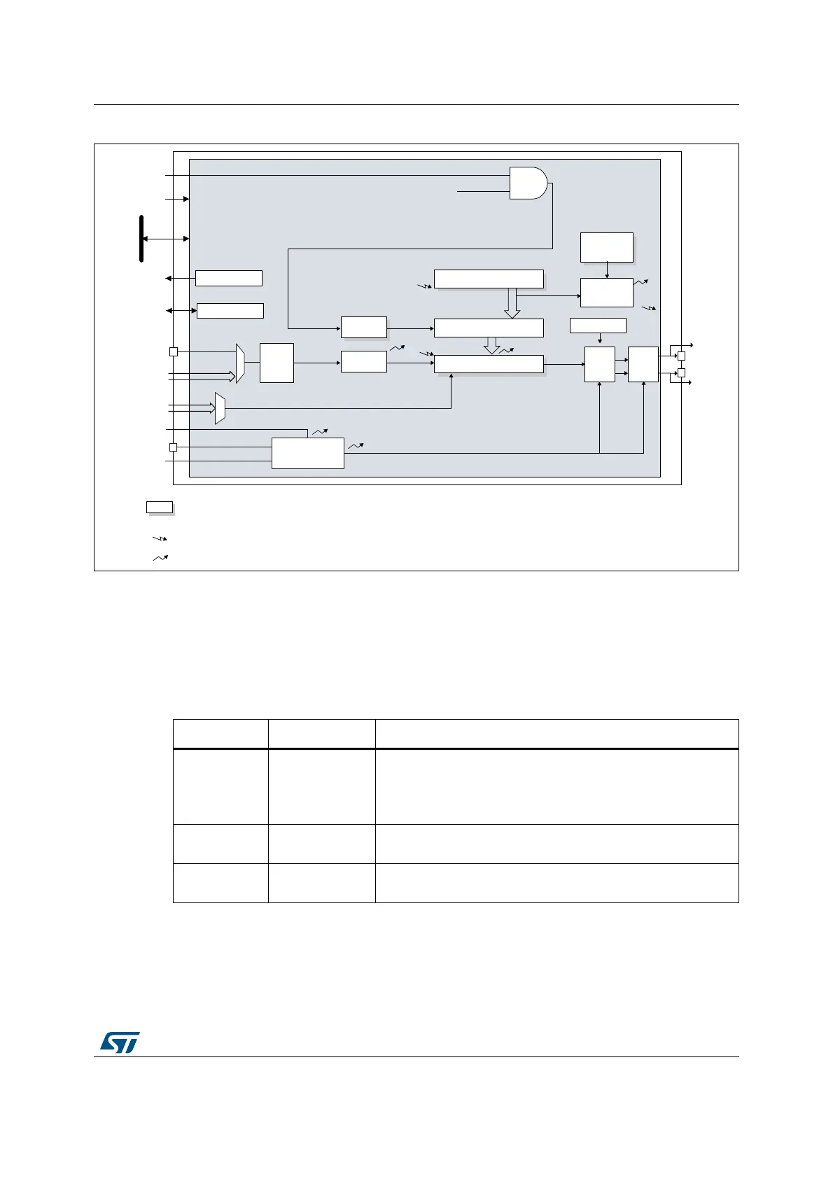
Figure 440. TIM16/TIM17 block diagram
1. Refer to Section 30.4.15: Using the break function for details.
2. This signal can be used as trigger for some slave timer (see internal trigger connection table in next section). See
Section 30.4.26: Using timer output as trigger for other timers (TIM16/TIM17) for details.
30.4.2 TIM15/TIM16/TIM17 pins and internal signals
Table 286 and Table 287 in this section summarize the TIM inputs and outputs.
MSv62372V3
tim_ker_ck
Counter Enable (CEN)
TIM_CH1
Auto-reload register
CNT counter
+/-
Capture/compare 1 register
tim_ti1fp1
tim_ic1
REP
register
Repetition
counter
DTG registers
DTG
Output
Control
tim_psc_ck
tim_cnt_ck
Stop, clear or up/down
tim_oc1ref
CC1I
C1I
U
UI
UEV
tim_oc
(2)
tim_oc1n
TIM_CH1
TIM_CH1N
Input
filter &
edge
detector
UEV
Notes:
Reg
Preload registers transferred
to active registers on U event
according to control bit
Event
Interrupt & DMA output
PSC
prescaler
Prescaler
tim_sys_brk
SBIF
Break circuitry
(1)
BIF
tim_brk
tim_ti1_in[1..15]
tim_ti1_in0
DMA interface
IRQ interface
tim_pclk
32-bit APB
bus
tim_cc1_dma
tim_upd_dma
tim_com_dma
tim_it
TIM_BKIN
tim_brk_cmp[7:1]
tim_ocref_clr_int
tim_ocref_clr[7..0]
Table 286. TIM input/output pins
Pin name Signal type Description
TIM_CH1
TIM_CH2
(1)
1. Available for TIM15 only.
Input/Output
Timer multi-purpose channels.
Each channel be used for capture, compare, or PWM.
TIM_CH1 and TIM_CH2 can also be used as external clock
(below 1/4 of the tim_ker_ck clock) and external trigger inputs.
TIM_CH1N Output
Timer complementary outputs, derived from TIM_CHx outputs
with the possibility to have deadtime insertion.
TIM_BKIN Input / Output
Break input. This input can also be configured in bidirectional
mode.
 Loading...


