FD controller area network (FDCAN) RM0440
1980/2126 RM0440 Rev 4
Note: With a CAN kernel clock of 48 MHz, the reset value of 0x06000A03 configures the FDCAN
for a bit rate of 3 MBit/s.
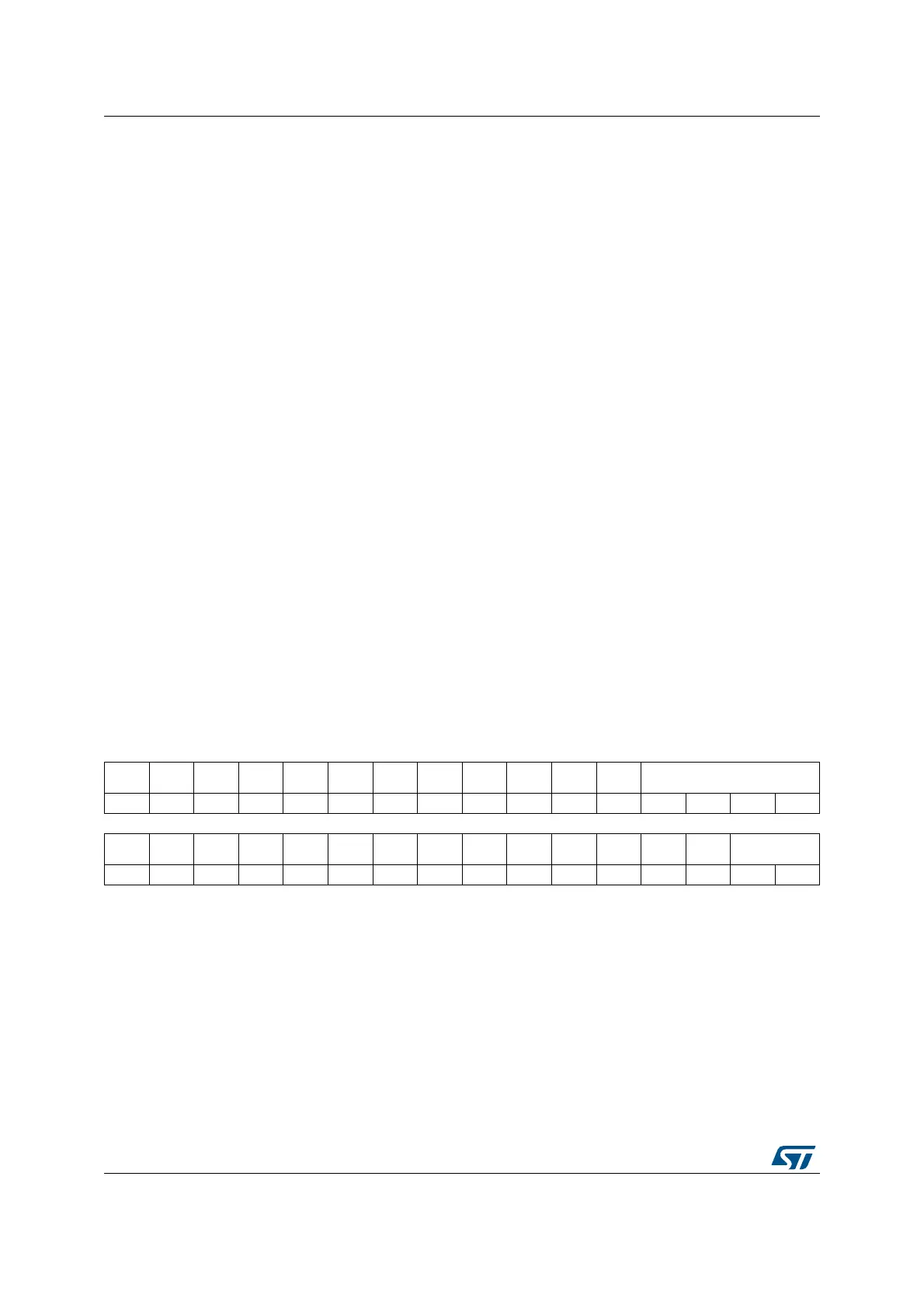
44.4.8 FDCAN timestamp counter configuration register (FDCAN_TSCC)
Address offset: 0x0020
Reset value: 0x0000 0000
Bits 31:25 NSJW[6:0]: Nominal (re)synchronization jump width
Valid values are 0 to 127. The actual interpretation by the hardware of this value is such that
the used value is the one programmed incremented by one.
These are protected write (P) bits, write access is possible only when the bit 1 [CCE] and bit
0 [INIT] of CCCR register are set to 1.
Bits 24:16 NBRP[8:0]: Bit rate prescaler
Value by which the oscillator frequency is divided for generating the bit time quanta. The bit
time is built up from a multiple of this quanta. Valid values are 0 to 511. The actual
interpretation by the hardware of this value is such that one more than the value programmed
here is used.
These are protected write (P) bits, write access is possible only when the bit 1 [CCE] and bit
0 [INIT] of CCCR register are set to 1.
Bits 15:8 NTSEG1[7:0]: Nominal time segment before sample point
Valid values are 0 to 255. The actual interpretation by the hardware of this value is such that
one more than the programmed value is used.
These are protected write (P) bits, write access is possible only when the bit 1 [CCE] and bit
0 [INIT] of CCCR register are set to 1.
Bit 7 Reserved, must be kept at reset value.
Bits 6:0 NTSEG2[6:0]: Nominal time segment after sample point
Valid values are 0 to 127. The actual interpretation by the hardware of this value is such that
one more than the programmed value is used.
31 30 29 28 27 26 25 24 23 22 21 20 19 18 17 16
Res. Res. Res. Res. Res. Res. Res. Res. Res. Res. Res. Res. TCP[3:0]
rw rw rw rw
1514131211109876543210
Res. Res. Res. Res. Res. Res. Res. Res. Res. Res. Res. Res. Res. Res. TSS[1:0]
rw rw
 Loading...


