RM0440 Rev 4 549/2126
RM0440 Flexible static memory controller (FSMC)
571
19.6.6 NOR/PSRAM controller registers
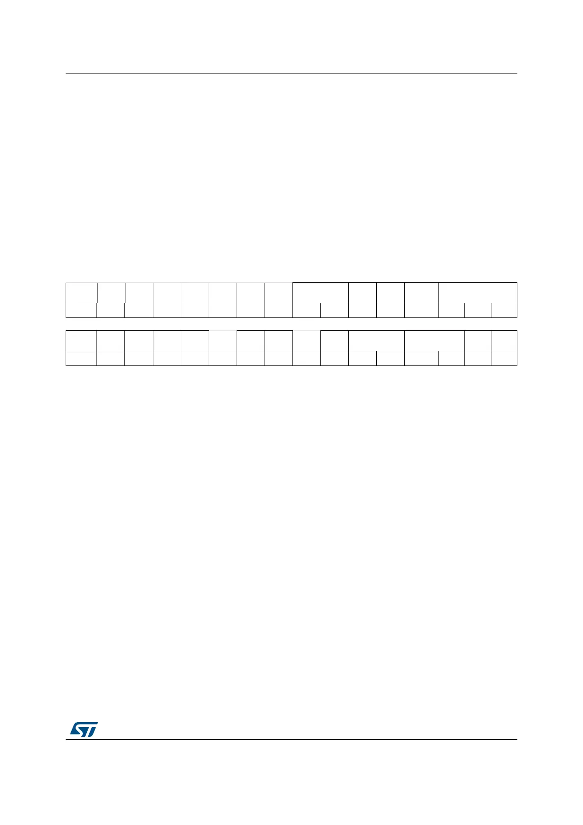
SRAM/NOR-Flash chip-select control register for bank x
(FMC_BCRx) (x = 1 to 4)
Address offset: 8 * (x – 1), (x = 1 to 4)
Reset value: Bank 1: 0x0000 30DB
Reset value: Bank 2: 0x0000 30D2
Reset value: Bank 3: 0x0000 30D2
Reset value: Bank 4: 0x0000 30D2
This register contains the control information of each memory bank, used for SRAMs,
PSRAM, FRAM and NOR Flash memories.
31 30 29 28 27 26 25 24 23 22 21 20 19 18 17 16
Res. Res. Res. Res. Res. Res. Res. Res. NBLSET[1:0] WFDIS
CCLK
EN
CBURST
RW
CPSIZE[2:0]
rw rw rw rw rw rw rw rw
15 14 13 12 11 10 9 8 7 6 5 4 3 2 1 0
ASYNC
WAIT
EXT
MOD
WAIT
EN
WREN
WAIT
CFG
Res.
WAIT
POL
BURST
EN
Res.
FACC
EN
MWID[1:0] MTYP[1:0]
MUX
EN
MBK
EN
rw rw rw rw rw rw rw rw rw rw rw rw rw rw
Bits 31:24 Reserved, must be kept at reset value.
Bits 23:22 NBLSET[1:0]: Byte lane (NBL) setup
These bits configure the NBL setup timing from NBLx low to chip select NEx low.
00: NBL setup time is 0 AHB clock cycle
01: NBL setup time is 1 AHB clock cycle
10: NBL setup time is 2 AHB clock cycles
11: NBL setup time is 3 AHB clock cycles
Bit 21 WFDIS: Write FIFO disable
This bit disables the Write FIFO used by the FMC controller.
0: Write FIFO enabled (Default after reset)
1: Write FIFO disabled
Note: The WFDIS bit of the FMC_BCR2..4 registers is don’t care. It is only enabled through the
FMC_BCR1 register.
 Loading...


