Sun Microelectronics
82
UltraSPARC User’s Manual
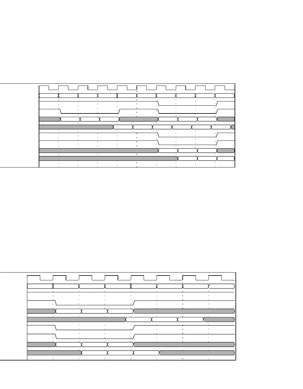
Figure 7-7 Timing for Coherent Writes with E-to-M State Transition (1–1–1 Mode)
Otherwise, the tag port is available for a tag check of a younger store during the
data write. In the timing diagram shown in Figure 7-5 on page 81, the store buffer
is empty when the first write request is made, which is why there is no overlap
between the tag accesses and the write accesses. In normal operation, if the line is
in M state, the tag access for one write can be done in parallel with the data write
of previous write (E state updates cannot be overlapped). This independence of
the tag and data buses make the peak store bandwidth as high as the load band-
width (one per cycle). Figure 7-8 shows the 1–1–1 Mode overlap of tag and data
accesses. The data for three previous writes (W0, W1 and W2) is written while
three tag accesses (reads) are made for three younger stores (R3, R4 and R5).
Figure 7-8 Timing Overlap: Tag Access / Data Write for Coherent Writes (1–1–1 Mode)
If the line is in Shared (S) or Owned (O) state, a read for ownership is performed
before writing the data.
CLK
CYCLE
0123456789
TSYN_WR_L
R0 R1 R2 U0 U1 U2
TOE_L
R0 R1 R2 U0 U1 U2
ECAT
A0_tag A1_tag A2_tag
TDATA
D0_tag D1_tag D2_tag
DSYN_WR_L
W0 W1 W2
DOE_L
W0 W1 W2
ECAD
A0_data A1_data A2_data
EDATA
D0_data D1_data D2_data
D0_tag D1_tag D2_tag
A0_tag A1_tag A2_tag
CLK
CYCLE 01234567
TSYN_WR_L R3 R4 R5
TOE_L R3 R4 R5
ECAT A3_tag A4_tag A5_tag
TDATA D3_tag D4_tag D5_tag
DSYN_WR_L W0 W1 W2
DOE_L W0 W1 W2
ECAD A0_data A1_data A2_data
EDATA D0_data D1_data D2_data
Artisan Technology Group - Quality Instrumentation ... Guaranteed | (888) 88-SOURCE | www.artisantg.com
 Loading...