Analog-to-Digital Converter
6 - 4 C2000 Microcontroller Workshop - Analog-to-Digital Converter
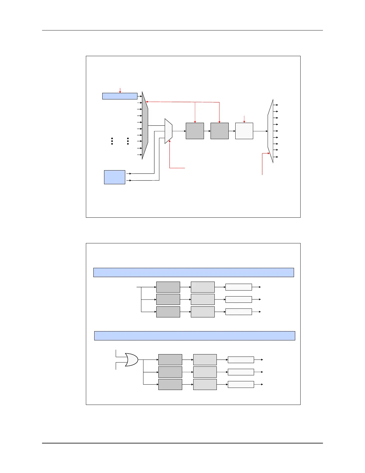
ADC SOCx Functional Diagram
This block diagram is replicated 16 times
Software Trigger
TINT0 (CPU Timer 0)
TINT1 (CPU Timer 1)
TINT2 (CPU Timer 2)
XINT2_ADCSOC (GPIO)
SOCA (ePWM1)
SOCB (ePWM1)
SOCA (ePWM8)
SOCB (ePWM8)
T
r
i
g
g
e
r
ADCINT1
ADCINT2
Re-Trigger
ADCINT1
ADCINT2
ADCINT3
ADCINT4
ADCINT5
ADCINT6
ADCINT7
ADCINT8
ADCINT9
Channel
Select
Sample
Window
Result
Register
S
O
C
x
E
O
C
x
ADCSOCxCTL
ADCSOCFRC1
ADCINTSOCSEL1
ADCINTSOCSEL2
INTSELxNy
ADCRESULTx
ADC Triggering
Example – ADC Triggering
(sequential sampling)
Sample A2
B3
A7 when ePWM1 SOCB is generated and then generate ADCINT1:
Channel
A2
Sample
7 cycles
Result0
Channel
B3
Sample
10 cycles
Result1
Channel
A7
Sample
8 cycles
Result2
SOC0
SOC1
SOC2
no interrupt
no interrupt
ADCINT1
SOCB (ETPWM1)
Then after above, sample A0
B0
A5 continuously and generate ADCINT2:
Channel
A0
Sample
10 cycles
Result3
Channel
B0
Sample
15 cycles
Result4
Channel
A5
Sample
12 cycles
Result5
SOC3
SOC4
SOC5
no interrupt
no interrupt
ADCINT2
ADCINT2
Software Trigger
The top example on this slide shows channels A2, B3, and A7 being converted with a trigger
from EPWM1SOCB. After A7 is converted, ADCINT1 is generated.