Memory
C2000 Microcontroller Workshop - Architecture Overview 1 - 9
Memory
The memory space on the F28x is divided into program memory and data memory. There are
several different types of memory available that can be used as both program memory and data
memory. They include the flash memory, single access RAM (SARAM), OTP, and Boot ROM
which is factory programmed with boot software routines and standard tables used in math related
algorithms.
Memory Map
The F28x CPU contains no memory, but can access memory on chip. The F28x uses 32-bit data
addresses and 22-bit program addresses. This allows for a total address reach of 4G words (1
word = 16-bits) in data memory and 4M words in program memory. Memory blocks on all F28x
designs are uniformly mapped to both program and data space.
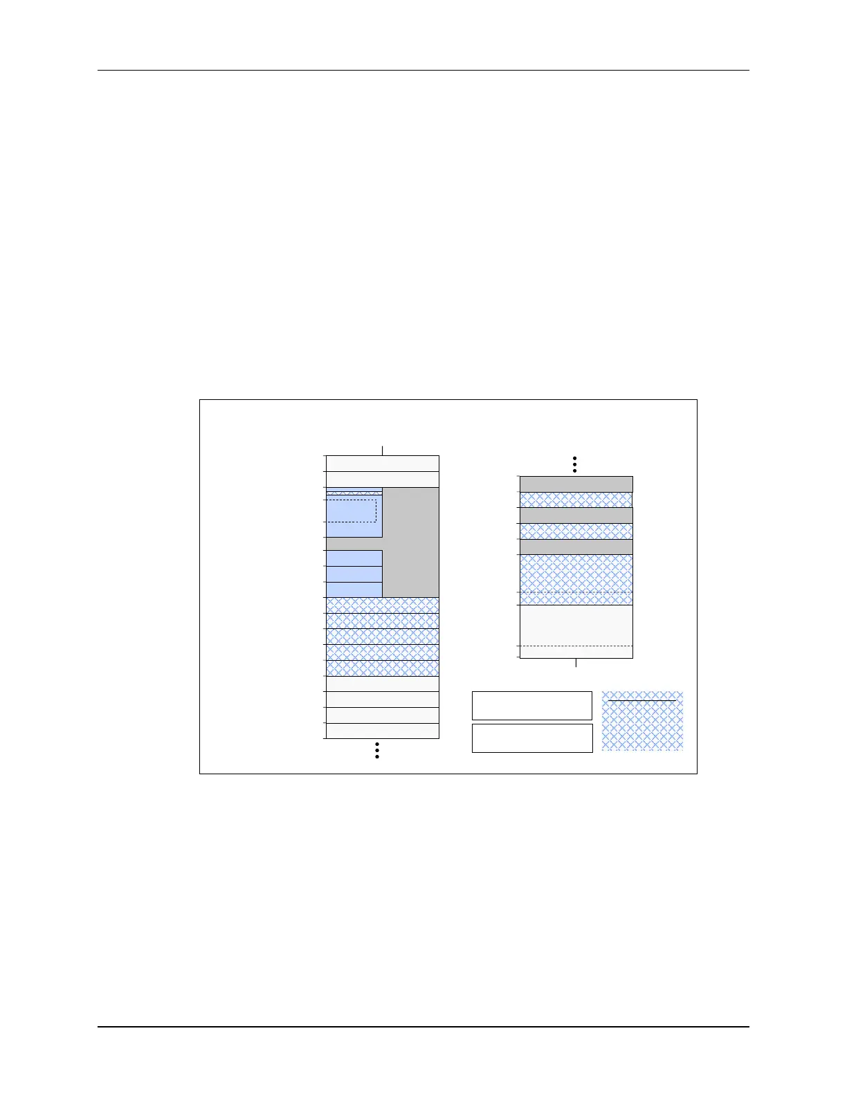
This memory map shows the different blocks of memory available to the program and data space.
TMS320F28069 Memory Map
0x000000
0x000400
0x000800
M1 SARAM (1Kw)
M0 SARAM (1Kw)
Data Program
PIE Vectors
(256 w)
PF 0 (6Kw)
reserved
PF 3 (4Kw)
PF 1 (4Kw)
L0 DPSARAM (2Kw)
L1 DPSARAM (1Kw)
L2 DPSARAM (1Kw)
L3 DPSARAM (4Kw)
0x000D00
0x002000
0x005000
0x006000
0x008000
0x008800
0x008C00
0x00A000
0x000E00
0x009000
reserved
Data Program
FLASH (128Kw)
PASSWORDS (8w)
0x3D7CC0
0x3D7C80
0x3D8000
Boot ROM (32Kw)
0x3F7FF8
0x3F8000
0x3FFFFF
CSM Protected:
L0, L1, L2, L3, L4,
OTP, FLASH,
ADC CAL,
Flash Regs in PF0
0x3FFFC0
BROM Vectors (64w)
ADC / OSC cal. data
DPSARAM L0, L1, L2 & L3
accessible by CPU & CLA
PF 2 (4Kw)
0x007000
0x014000
0x3D7800
0x3D7C00
User OTP (1Kw)
reserved
reserved
L4 SARAM (8Kw)
L5 DPSARAM (8Kw)
L6 DPSARAM (8Kw)
L7 DPSARAM (8Kw)
0x00C000
0x00E000
0x012000
0x010000
L8 DPSARAM (8Kw)
0x014000
DPSARAM L5, L6, L7 & L8
accessible by DMA
The F28069 utilizes a contiguous memory map, also known as a von-Neumann architecture. This
type of memory map lends itself well to higher-level languages. This can be seen by the labels
located at the top of the memory map where the memory blocks extend between both the data
space and program space.
At the top of the map, we have two blocks of RAM called M0 and M1. Then we see PF0 through
PF3, which are the peripheral frames. This is the area where you will find the peripheral
registers. Also in this space, you will find the PIE block. Memory blocks L0 through L8 are
grouped together. L0 through L3 are accessible by the CPU and CLA. L5 through L8 are
accessible by the DMA.