What is the TMS320C2000™?
1 - 4 C2000 Microcontroller Workshop - Architecture Overview
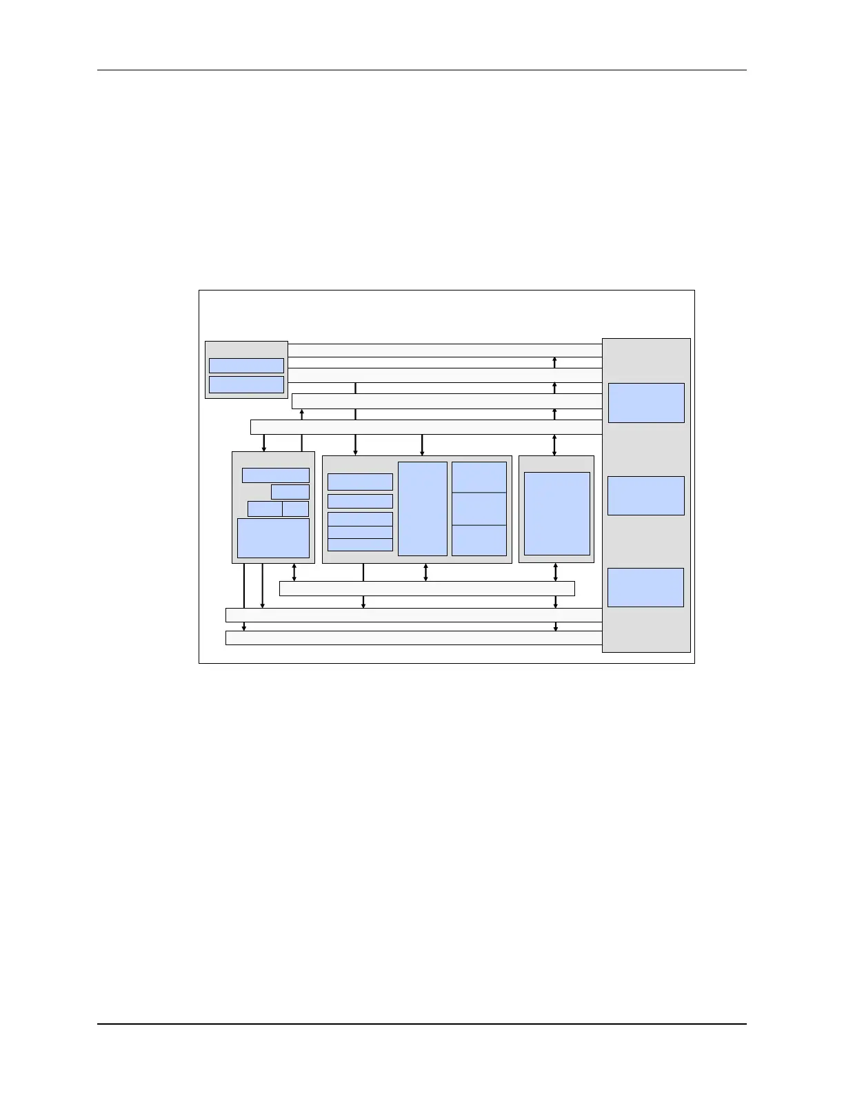
TMS320C2000™ Internal Bussing
As with many DSP-type devices, multiple busses are used to move data between the memories
and peripherals and the CPU. The F28x memory bus architecture contains:
• A program read bus (22-bit address line and 32-bit data line)
• A data read bus (32-bit address line and 32-bit data line)
• A data write bus (32-bit address line and 32-bit data line)
Program-read Data Bus (32)
F28x CPU Internal Bus Structure
Data-write Address Bus (32)
Program Address Bus (22)
Execution
R-M-W
Atomic
ALU
Real-Time
JTAG
Emulation
Program
Decoder
PC
XAR0
to
XAR7
SP
DP @X
ARAU
MPY32x32
XT
P
ACC
ALU
Registers
Debug
Register Bus / Result Bus
Data/Program-write Data Bus (32)
Data-read Address Bus (32)
Data-read Data Bus (32)
FPU
R0H-R7H
Program
Memory
Data
Memory
Peripherals
VCU
VR0-VR8
CLA
MR0-MR3
The 32-bit-wide data busses provide single cycle 32-bit operations. This multiple bus
architecture, known as a Harvard Bus Architecture, enables the F28x to fetch an instruction, read
a data value and write a data value in a single cycle. All peripherals and memories are attached to
the memory bus and will prioritize memory accesses.