General-Purpose Digital I/O
5 - 12 C2000 Microcontroller Workshop - System Initialization
General-Purpose Digital I/O
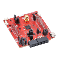
F2806x GPIO Grouping Overview
(lab file: Gpio.c)
GPIO Port A Mux1
Register (GPAMUX1)
[GPIO 0 to 15]
GPIO Port A
Direction Register
(GPADIR)
[GPIO 0 to 31]
GPIO Port A
GPIO Port B
Internal Bus
GPIO Port A Mux2
Register (GPAMUX2)
[GPIO 16 to 31]
GPIO Port B Mux1
Register (GPBMUX1)
[GPIO 32 to 47]
GPIO Port B
Direction Register
(GPBDIR)
[GPIO 32 to 63]
ANALOG Port
ANALOG I/O Mux1
Register (AIOMUX1)
[AIO 0 to 15]
ANALOG Port
Direction Register
(AIODIR)
[AIO 0 to 15]
Input
Qual
Input
Qual
GPIO Port B Mux2
Register (GPBMUX2)
[GPIO 48 to 63]
Each general-purpose I/O pin has a maximum of four options, either general-purpose I/O or up to
three possible peripheral pin assignments. This is selected using the GPIO port multiplexer. If
the pin is set to GPIO, the direction register sets it as an input or an output. The input
qualification will be explained shortly.
•
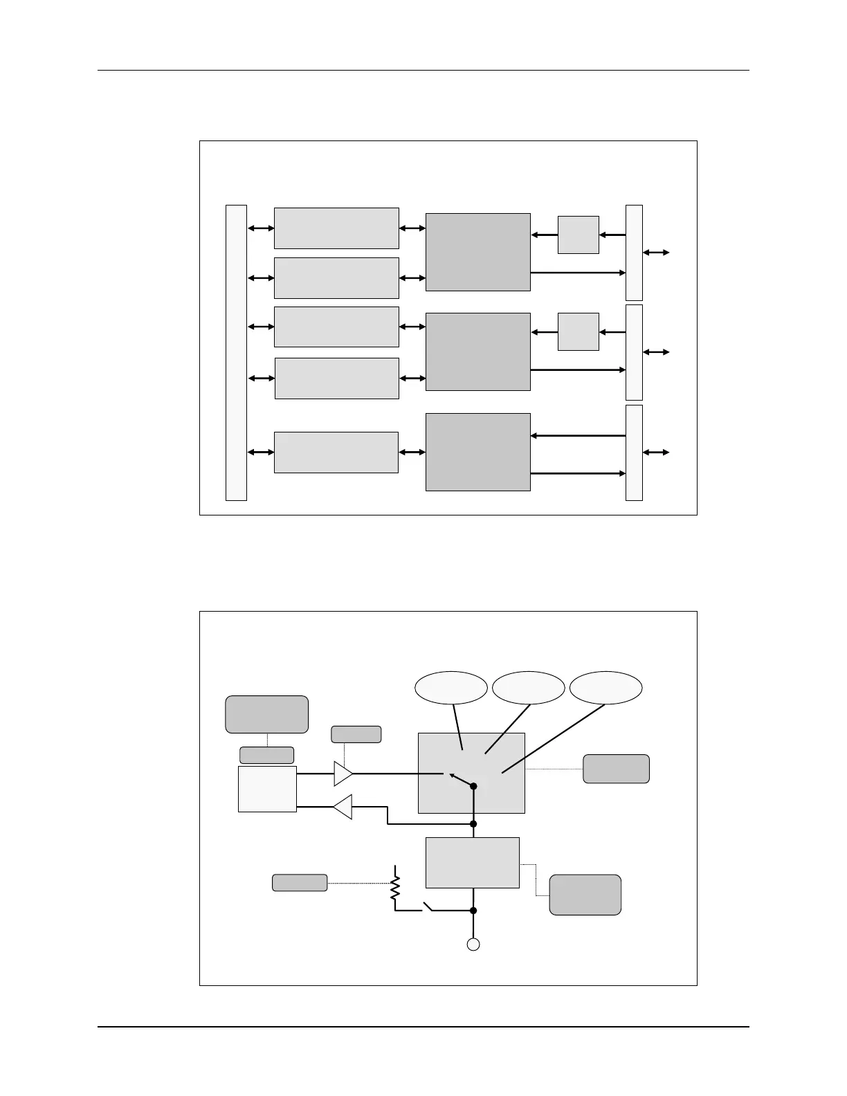
F2806x GPIO Pin Block Diagram
(lab file: Gpio.c)
• •
01
00
MUX Control Bits *
00 = GPIO
01 = Peripheral 1
10 = Peripheral 2
11 = Peripheral 3
Peripheral
1
I/O DAT
Bit (R/W)
In
Out
I/O DIR Bit
0 = Input
1 = Output
GPxMUX1
GPxMUX2
GPxDIR
GPxDAT
GPxSET
GPxCLEAR
GPxTOGGLE
••
10
11
Peripheral
2
Peripheral
3
Pin
Internal Pull-Up
0 = enable (default GPIO 12-58)
1 = disable (default GPIO 0-11)
GPxPUD
Input
Qualification
(GPIO 0-44)
GPxQSEL1
GPxQSEL2
GPxCTRL
* See device datasheet for pin function selection matrices