Lab 6: Analog-to-Digital Converter
6 - 20 C2000 Microcontroller Workshop - Analog-to-Digital Converter
This buffer pointer will be managed in a circular fashion, such that new conversion results will
continuously overwrite older conversion results in the buffer. In order to generate an interesting
input signal, the code also alternately toggles a GPIO pin (GPIO18) high and low in the ADC
interrupt service routine. The ADC ISR will also toggle LED LD3 on the controlCARD as a
visual indication that the ISR is running. This pin will be connected to the ADC input pin, and
sampled. After taking some data, Code Composer Studio will be used to plot the results. A flow
chart of the code is shown in the following slide.
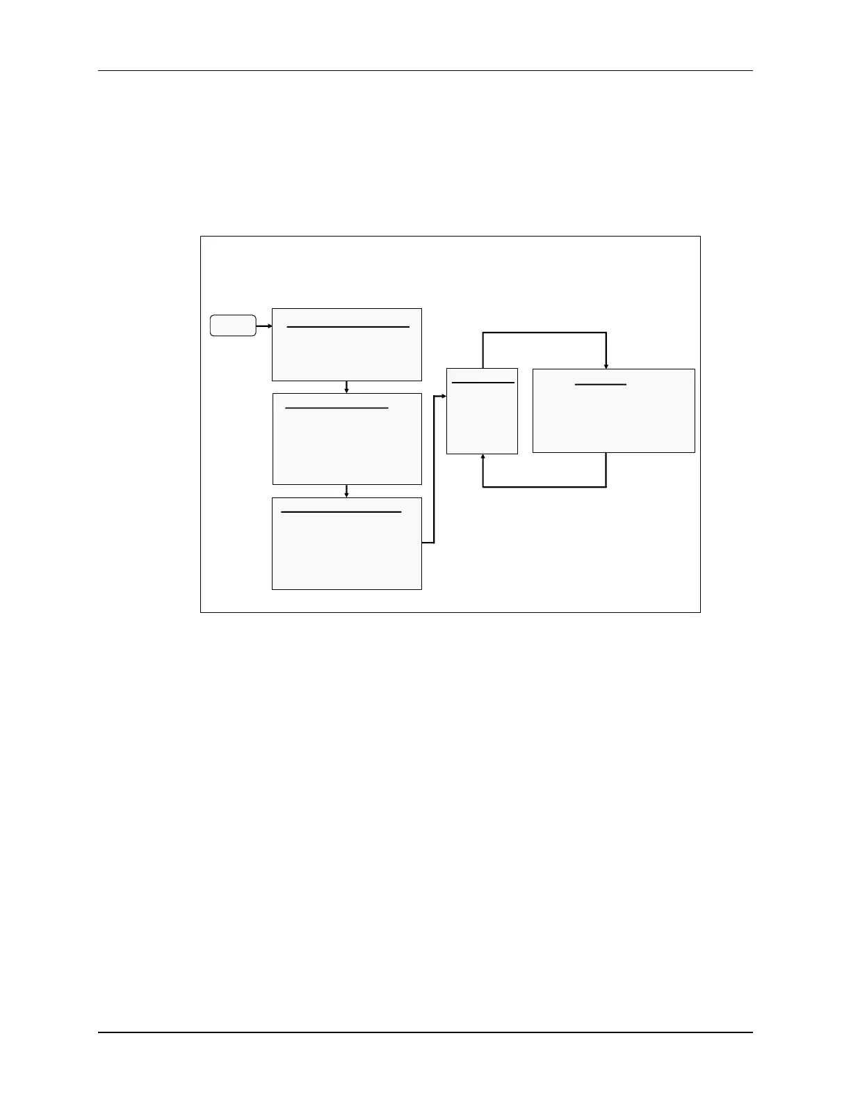
Lab 6: Code Flow Diagram
Start
General Initialization
• PLL and clocks
•
watchdog
configure
• GPIO setup
• PIE initialization
ADC Initialization
• convert channel A0 on
ePWM2 period match
• send interrupt on EOC
to trigger ADC ISR
• setup a results buffer
in memory
ePWM2 Initialization
• clear counter
• set period register
• set to trigger ADC on
period match
• set the clock prescaler
• enable the timer
Main Loop
while(1)
{
}
ADC ISR
• read the ADC result
• write to result buffer
• adjust the buffer pointer
• toggle the GPIO pin
• return from interrupt
ADC interrupt
return
Notes
• Program performs conversion on ADC channel A0 (ADCINA0 pin)
• ADC conversion is set at a 50 kHz sampling rate
• ePWM2 is triggering the ADC on period match using SOCA trigger
• Data is continuously stored in a circular buffer
• GPIO18 pin is also toggled in the ADC ISR
• ADC ISR will also toggle the controlCARD LED LD3 as a visual indication that it is running
 Loading...


