– 2.4 –
2-1-2. Power supply
Input/output of the power supply are as follows:
Input: 100 VAC to 240 VAC, 50/60 Hz
Output: +3.3 V, 3.5 A
+5 V, 3.5 A
+35 V, 6 A
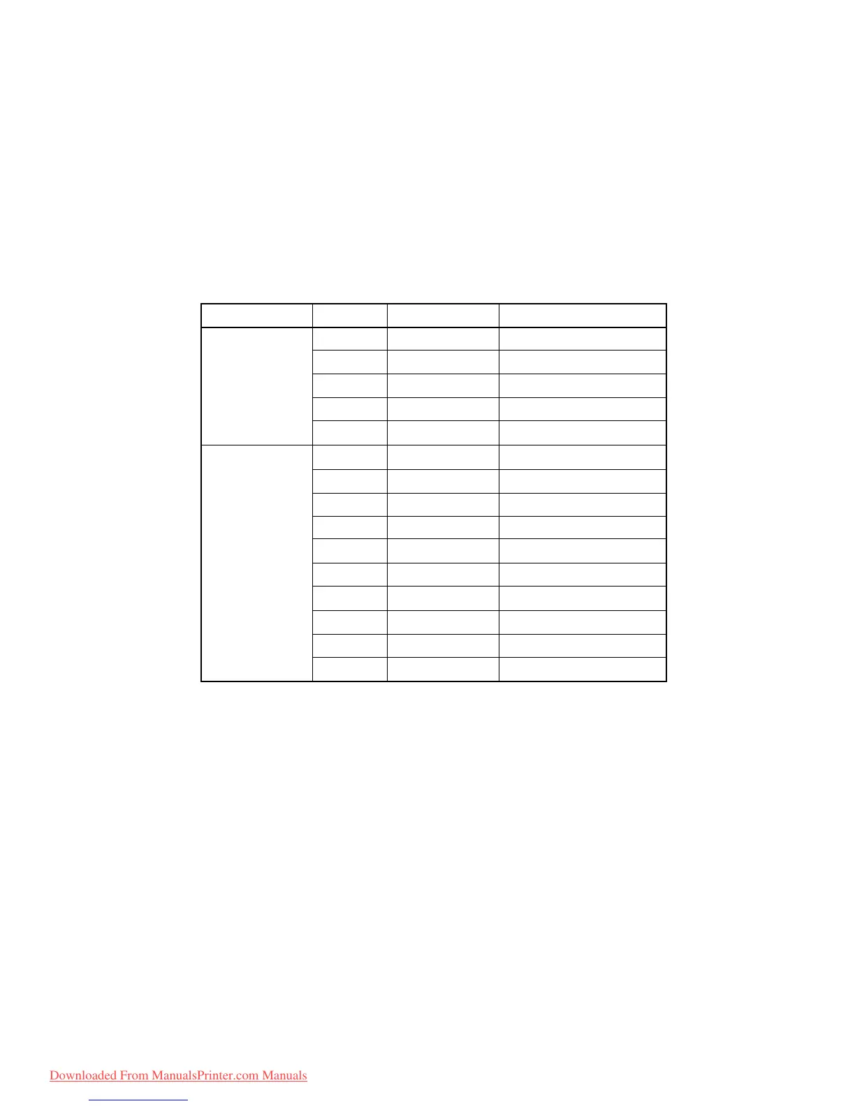
Connector pins layout table and variable resistor numbers
Connector Pin No. Name of signal Variable resistor
CN1 1 NC
2NC
3 AC IN (L)
4NC
5 AC IN (N)
CN2 1 +35V RV1 (CN2 proximity)
2 +35V
3 GND
4 GND
5 +5V RV2 (CN2 proximity)
6 +5V
7 GND
8 GND
9 +3.3V RV3 (CN2 proximity)
10 +3.3V
2-1-3. Main PCB
The SH-3 (RISC, 133MHz) from Hitachi is used as the CPU.
The program of the CPU is stored in the flash memory. This program can easily be upgraded
on site through the interface.
During upgrading, the program is downloaded to the PRAM by the CPU and then stored in
the flash memory of the CPU.
When the receive data is read from the interface, the CPU loads the data in the picture memory
through the PDC-CTR. The picture memory consists of a 256MB DSRAM.
The PDC-CTR performs necessary mask processing, performs X-Y conversion, then transfers
it to the head controller (on the HDC PCB) with 8-bit width.
Downloaded From ManualsPrinter.com Manuals
 Loading...