137
CHAPTER 6 PORT FUNCTIONS
P-ch
WR
PM
WR
PORT
RD
WR
PUO
V
DD
Selector
PUO2
Output Latch
(P20, P21, P23-P26)
PM20, PM21
PM23-PM26
Internal bus
Alternate Function
P20/SI1,
P21/SO1,
P23/STB,
P24/BUSY,
P25/SI0/SB0,
P26/SO0/SB1
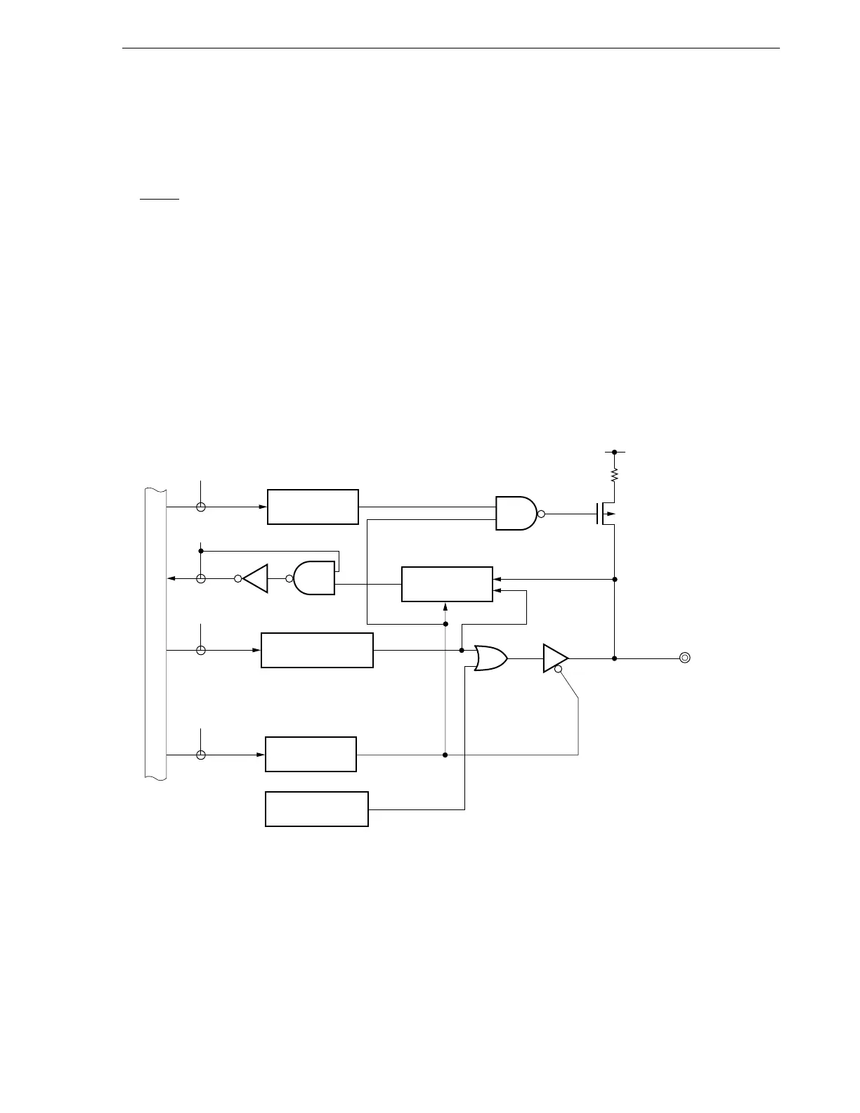
6.2.3 Port 2 (
µ
PD78054 Subseries)
Port 2 is an 8-bit input/output port with output latch. P20 to P27 pins can specify the input mode/output mode in
1-bit units with the port mode register 2 (PM2). When P20 to P27 pins are used as input ports, an on-chip pull-up
resistor can be used to them in 8-bit units with a pull-up resistor option register L (PUOL).
Alternate functions include serial interface data input/output, clock input/output, automatic transmit/receive busy
input, and strobe output.
RESET input sets port 2 to input mode.
Figures 6-5 and 6-6 show block diagrams of port 2.
Cautions 1. When used as a serial interface, set the input/output and output latch according to its
functions. For the setting method, refer to Figure 16-4 Serial Operating Mode Register 0
Format and Figure 18-3 Serial Operating Mode Register 1 Format.
2. When reading the pin state in SBI mode, set PM2n bit of PM2 to 1 (n = 5, 6) (Refer to the
description of (10) Discrimination of slave busy state in section 16.4.3 “SBI Mode
Operation”).
Figure 6-5. P20, P21, P23 to P26 Block Diagram
PUO : Pull-up resistor option register
PM : Port mode register
RD : Port 2 read signal
WR : Port 2 write signal