473
CHAPTER 19 SERIAL INTERFACE CHANNEL 2
(3) MSB/LSB switching as the start bit
The 3-wire serial I/O mode enables to select transfer to start from MSB or LSB.
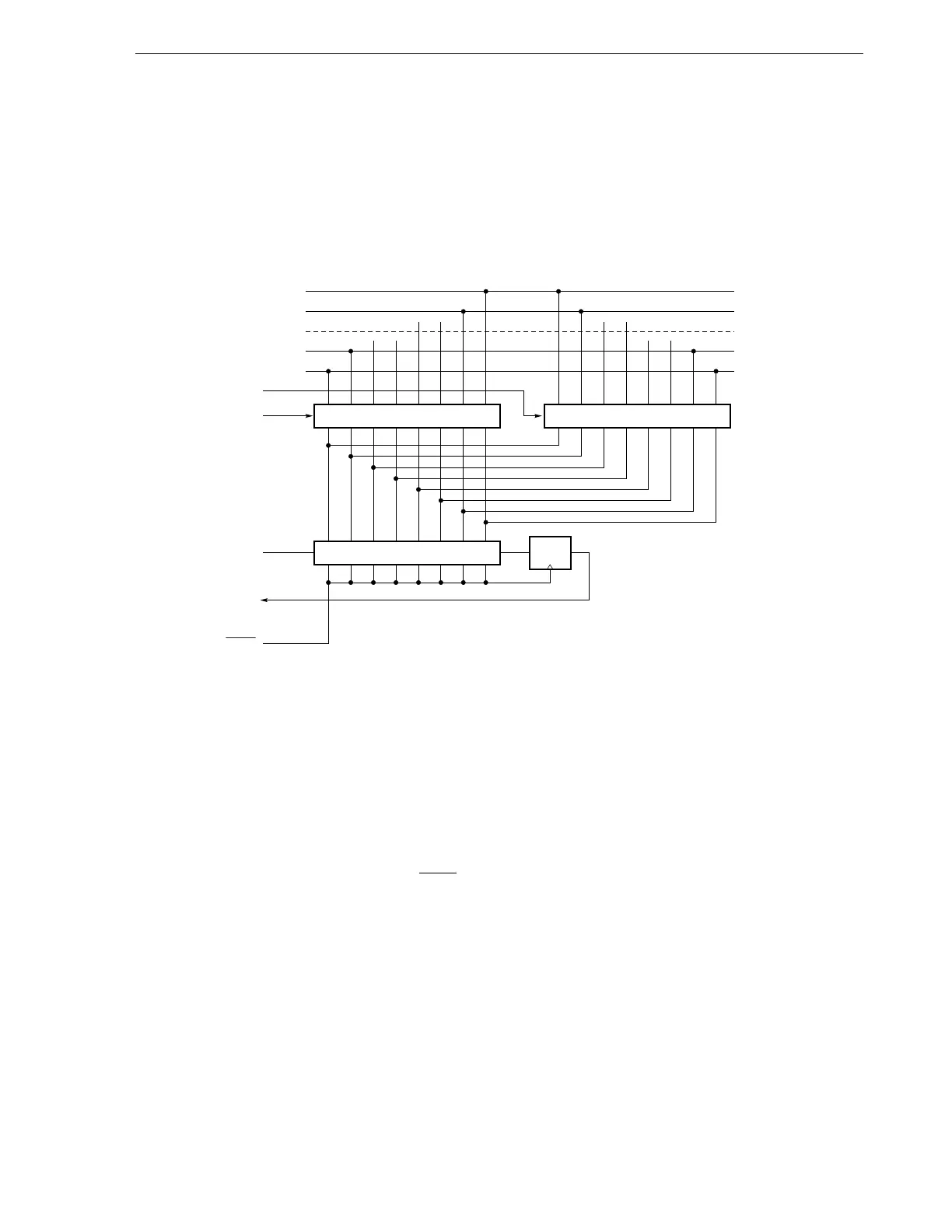
Figure 19-13 shows the configuration of the transmit shift register (TXS/SIO2) and internal bus. As shown
in the figure, MSB/LSB can be read/written in reverse form.
MSB/LSB switching as the start bit can be specified with bit 2 (CSIM22) of the serial operating mode register
2 (CSIM2).
Figure 19-13. Circuit of Switching in Transfer Bit Order
Start bit switching is realized by switching the bit order for data write to TXS/SIO2. The TXS/SIO2 shift order
remains unchanged.
Thus, switching between MSB-first and LSB-first must be performed before writing data to the TXS/SIO2.
(4) Transfer start
Serial transfer is started by setting transfer data to the transmission shift register (TXS/SIO2) when the
following two conditions are satisfied.
• Serial interface channel 2 operation control bit (CSIE2) = 1
• Internal serial clock is stopped or SCK2 is a high level after 8-bit serial transfer.
Caution If CSIE2 is set to "1" after data write to TXS/SIO2, transfer does not start.
Upon termination of 8-bit transfer, serial transfer automatically stops and the interrupt request flag (SRIF) is
set.
7
6
Internal Bus
1
0
LSB-first
MSB-first Read/Write Gate
SI2
Transmit Shift Register (TXS/SIO2)
Read/Write Gate
SO2
SCK2
DQ
SO2 Latch