339
CHAPTER 16 SERIAL INTERFACE CHANNEL 0 (
µ
PD78054 Subseries)
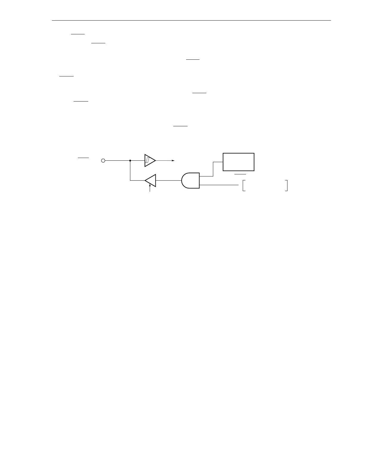
16.4.5 SCK0/P27 pin output manipulation
Because the SCK0/P27 pin incorporates an output latch, static output is also possible by software in addition to
normal serial clock output.
P27 output latch manipulation enables any value of SCK0 to be set by software. (SI0/SB0 and SO0/SB1 pin to
be controlled with the RELT and CMDT bits of serial bus interface control register (SBIC).)
SCK0/P27 pin output manipulating procedure is described below.
<1> Set the serial operating mode register 0 (CSIM0) (SCK0 pin enabled for serial operation in the output mode).
SCK0 = 1 with serial transfer suspended.
<2> Manipulate the P27 output latch with a bit manipulation instruction.
Figure 16-34. SCK0/P27 Pin Configuration
To Internal
Circuit
SCK0/P27
P27 Output
Latch
When CSIE0 = 1
and
CSIM01 and CSIM00 are 1 and 0, or 1 and 1.
SCK0 (1 while transfer is stopped)
From Serial Clock
Control Circuit
Manipulated by bit
manipulation instruction