142
CHAPTER 6 PORT FUNCTIONS
P40
P41
P42
P43
P44
P45
P46
P47
Falling Edge
Detection Circuit
KRMK
KRIF Set Signal
Standby Release
Signal
P-ch
WR
MM
WR
PORT
RD
WR
PUO
V
DD
Selector
PUO4
Output Latch
(P40 to P47)
MM
Internal bus
P40/AD0
P47/AD7
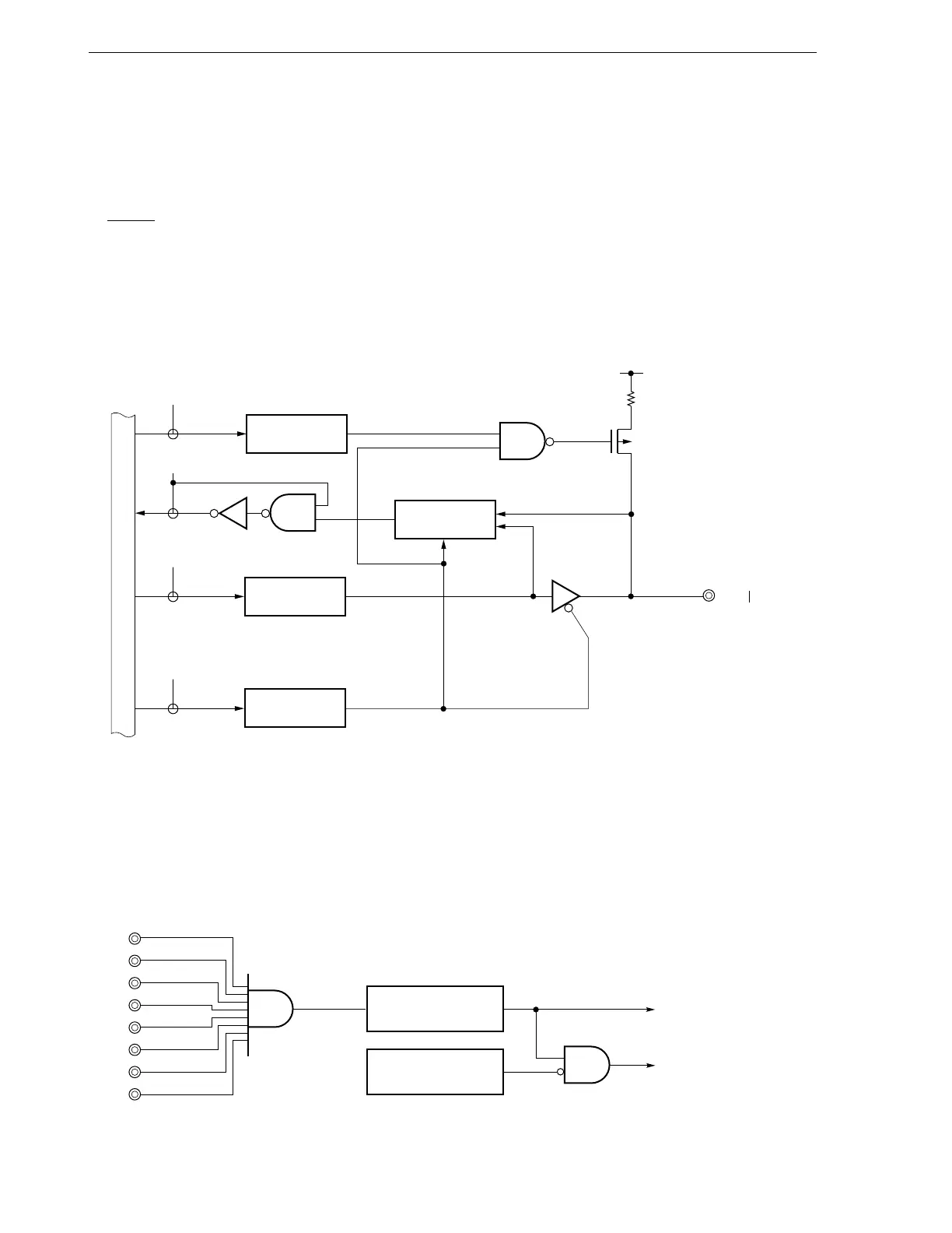
6.2.6 Port 4
Port 4 is an 8-bit input/output port with output latch. P40 to P47 pins can specify the input mode/output mode in
8-bit units with the memory expansion mode register (MM). When P40 to P47 pins are used as input ports, an on-
chip pull-up resistor can be used to them in 8-bit units with pull-up resistor option register L (PUOL).
The test input flag (KRIF) can be set to 1 by detecting falling edges.
Alternate function includes address/data bus function in external memory expansion mode.
RESET input sets port 4 to input mode.
Figures 6-10 and 6-11 show a block diagram of port 4 and block diagram of falling edge detection circuit,
respectively.
Figure 6-10. P40 to P47 Block Diagram
PUO : Pull-up resistor option register
MM : Memory expansion mode register
RD : Port 4 read signal
WR : Port 4 write signal
Figure 6-11. Block Diagram of Falling Edge Detection Circuit