VS 2001
Technical Handbook
Accessories
P/N: 779-0373/02
Revision 02
Marconi Proprietary information
Page 35
The equipment operates in Trunking Mode with zero switching time (Rx / Tx) within
the same frame, i.e. the equipment receives and transmits on adjacent slots.
• The R/T card contains the circuits listed below:
• Tuneable RF head and mixer for the first frequency conversion;
• First intermediate frequency with quartz filter;
• Second intermediate filter and low frequency;
• Circuits for base band reception, service circuits and interface circuits with the
Base Band card inherent in the reception section;
• Frequency synthesiser (a second synthesiser is been added);
• Power supply circuits (DC/DC converter), service circuits and interface circuits
with the Base Band card inherent in the transmission section;
• TX mixer. Tuneable filter and first amplifier;
• Second tuneable filter and second amplifier;
• Third amplifier and power reducer;
• Phase-shifter circuits to generate the modulating components;
• Transmission modulator;
• Demodulation circuits for the RF signal and feedback circuits for phase
correction.
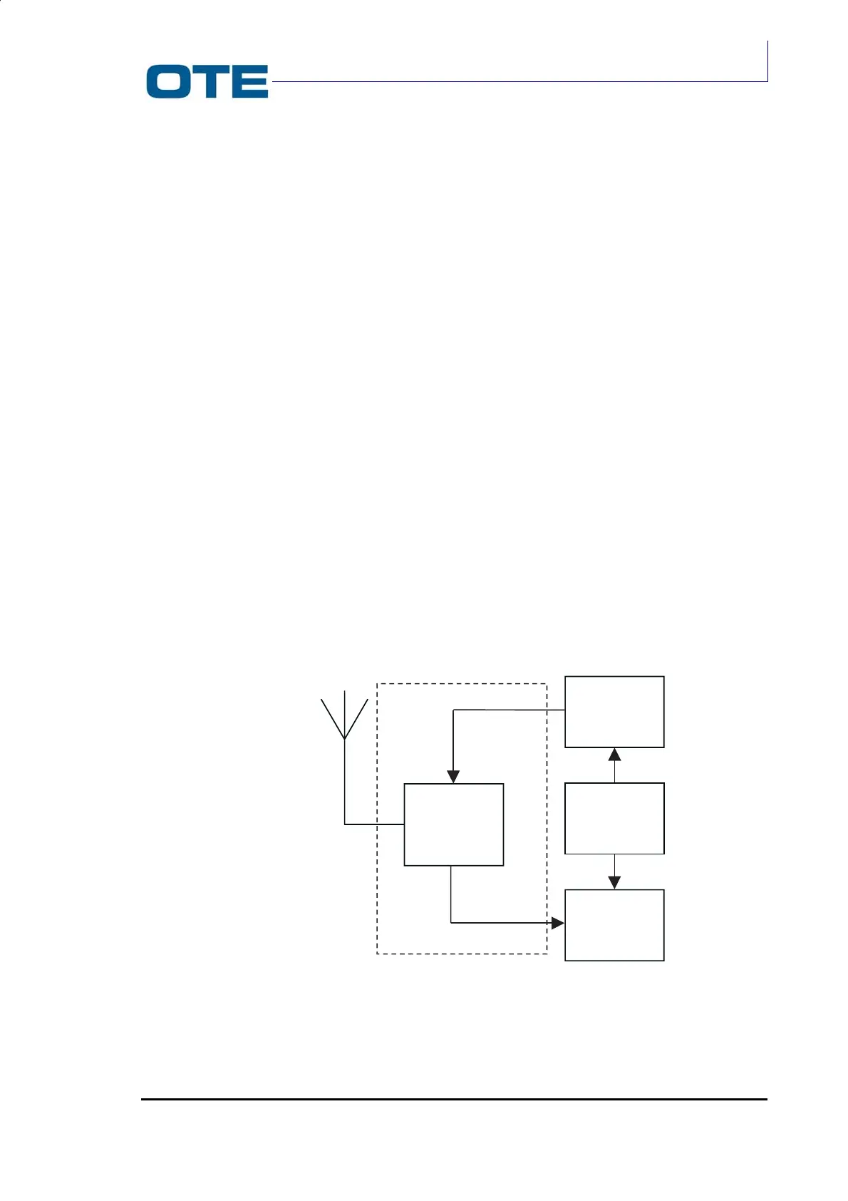
The block diagram of the R/T card RF section is shown in Fig. 2.8.
Fig. 2.8: RF section functional block diagram
F
TX
F
RX
LO
TX
LO
RX
ANTENNA
TX
SYNTH
TX/RX
RX
SW
PA
MODULE